MDS-JE770
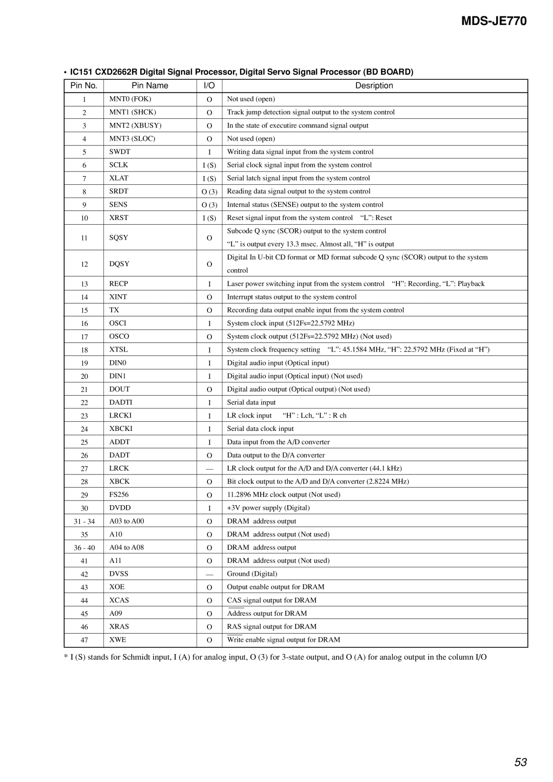
• IC151 CXD2662R Digital Signal Processor, Digital Servo Signal Processor (BD BOARD)
Pin No. | Pin Name | I/O |
|
|
|
| Desription |
|
|
|
|
|
|
|
|
1 | MNT0 (FOK) | O |
| Not used (open) | |||
|
|
|
|
| |||
2 | MNT1 (SHCK) | O |
| Track jump detection signal output to the system control | |||
|
|
|
|
|
|
|
|
3 | MNT2 (XBUSY) | O |
| In the state of executire command signal output | |||
|
|
|
|
|
|
|
|
4 | MNT3 (SLOC) | O |
| Not used (open) | |||
|
|
|
|
|
|
|
|
5 | SWDT | I |
| Writing data signal input from the system control | |||
|
|
|
|
|
|
|
|
6 | SCLK | I (S) |
| Serial clock signal input from the system control | |||
|
|
|
|
|
|
|
|
7 | XLAT | I (S) |
| Serial latch signal input from the system control | |||
|
|
|
|
|
|
|
|
8 | SRDT | O (3) |
| Reading data signal output to the system control | |||
|
|
|
|
|
|
|
|
9 | SENS | O (3) |
| Internal status (SENSE) output to the system control | |||
|
|
|
|
|
|
|
|
10 | XRST | I (S) |
| Reset signal input from the system control “L”: Reset | |||
|
|
|
|
|
|
|
|
11 | SQSY | O |
| Subcode Q sync (SCOR) output to the system control | |||
| “L” is output every 13.3 msec. Almost all, “H” is output | ||||||
|
|
|
| ||||
|
|
|
|
|
|
|
|
12 | DQSY | O |
| Digital In | |||
| control | ||||||
|
|
|
| ||||
|
|
|
|
|
|
|
|
13 | RECP | I |
| Laser power switching input from the system control “H”: Recording, “L”: Playback | |||
|
|
|
|
|
|
|
|
14 | XINT | O |
| Interrupt status output to the system control | |||
|
|
|
|
|
|
|
|
15 | TX | O |
| Recording data output enable input from the system control | |||
|
|
|
|
|
|
|
|
16 | OSCI | I |
| System clock input (512Fs=22.5792 MHz) | |||
|
|
|
|
|
|
|
|
17 | OSCO | O |
| System clock output (512Fs=22.5792 MHz) (Not used) | |||
|
|
|
|
|
|
|
|
18 | XTSL | I |
| System clock frequency setting “L”: 45.1584 MHz, “H”: 22.5792 MHz (Fixed at “H”) | |||
|
|
|
|
|
|
|
|
19 | DIN0 | I |
| Digital audio input (Optical input) | |||
|
|
|
|
|
|
|
|
20 | DIN1 | I |
| Digital audio input (Optical input) (Not used) | |||
|
|
|
|
|
|
|
|
21 | DOUT | O |
| Digital audio output (Optical output) (Not used) | |||
|
|
|
|
|
|
|
|
22 | DADTI | I |
| Serial data input | |||
|
|
|
|
|
|
|
|
23 | LRCKI | I |
| LR clock input “H” : Lch, “L” : R ch | |||
|
|
|
|
|
|
|
|
24 | XBCKI | I |
| Serial data clock input | |||
|
|
|
|
|
|
|
|
25 | ADDT | I |
| Data input from the A/D converter | |||
|
|
|
|
| |||
26 | DADT | O |
| Data output to the D/A converter | |||
|
|
|
|
|
|
|
|
27 | LRCK | — |
| LR clock output for the A/D and D/A converter (44.1 kHz) | |||
|
|
|
|
|
|
|
|
28 | XBCK | O |
| Bit clock output to the A/D and D/A converter (2.8224 MHz) | |||
|
|
|
|
|
|
|
|
29 | FS256 | O |
| 11.2896 MHz clock output (Not used) | |||
|
|
|
|
|
|
|
|
30 | DVDD | I |
| +3V power supply (Digital) | |||
|
|
|
|
| |||
31 - 34 | A03 to A00 | O |
| DRAM address output | |||
35 | A10 | O |
| DRAM address output (Not used) | |||
36 - 40 | A04 to A08 | O |
| DRAM address output | |||
|
|
|
|
|
|
|
|
41 | A11 | O |
| DRAM address output (Not used) | |||
|
|
|
|
|
|
|
|
42 | DVSS | — |
| Ground (Digital) | |||
|
|
|
|
|
|
|
|
43 | XOE | O |
| Output enable output for DRAM | |||
|
|
|
|
|
|
|
|
44 | XCAS | O |
| CAS signal output for DRAM | |||
|
|
|
|
|
|
|
|
|
|
|
|
|
|
| |
45 | A09 | O |
| Address output for DRAM | |||
46 | XRAS | O |
| RAS signal output for DRAM | |||
|
|
|
|
|
|
| |
|
|
|
|
|
|
|
|
47 | XWE | O |
| Write enable signal output for DRAM | |||
|
|
|
|
|
|
|
|
* I (S) stands for Schmidt input, I (A) for analog input, O (3) for
53