Manuals
/
Sony
/
Home Audio
/
CD Player
Sony
MZ-R90/R91, MT-MZR70-165
service manual
Models:
MT-MZR70-165
MZ-R90/R91
1
38
51
51
Download
51 pages
22.19 Kb
35
36
37
38
39
40
41
42
Parts list
Diagrams
Connecting Location
Section Disassembly
Section Electrical Adjustments
Service Assy, Op
Page 38
Image 38
Page 37
Page 39
Page 38
Image 38
Page 37
Page 39
Contents
AEP Model
US Model
Canadian Model
UK Model
Flexible Circuit Board Repairing
Notes on chip component replacement
TABLE OF CONTENTS
NOTES ON HANDLING THE OPTICAL PICK-UPBLOCK LCX-2R
SECTION SERVICING NOTE
NOTES ON LASER DIODE EMISSION CHECK
OPTICAL PICK-UPFLEXIBLE BOARD
SECTION 2 GENERAL
Page
Page
SECTION DISASSEMBLY
3-3.LCD MODULE
3-4.MAIN BOARD
over write head section
3-6.SERVICE ASSY, OP
3-5.MD MECHANISM DECK MT-MZR70-165
3-7.HOLDER ASSY
3-8.MOTOR FLEXIBLE BOARD
3-9.MOTOR, DC M602
3-10.“MOTOR, DC M601”, “MOTOR, DC M603”
4-2-1.Setting Method of Test Mode
SECTION 4 TEST MODE
4-2-2.Operation in Setting the Test Mode
888xxxxxxxxxFREC1SHUF
000M a n u a l
011 0 6 3 B
011 C 6 8 S
011 0 F FJ
011 0 5 9 A
000S t a t 000A d r s 000B E m p 000# # # # # #
000P * * R
E I B
000P * * R 000B O v r 000B f u l 000R t r y
000N - 1 000N - 1 000N - 2 000N - 2 000N
0001 s t
0001 s t 0001 s t 0001 s t
000R # # # #
Description of Error Indication Codes
• Description of Indication History
4-7.KEY CHECK MODE
021R e s O K ?
SECTION ELECTRICAL ADJUSTMENTS
021R e s N
021R e s
763V r h V c l
762V c l P W M
765V c h P W M
766V r h V c h
C D R U N
014S e t T m p
000 A s s y
341 C D O K
Connection
043R e s u m e
043R e s C l r
Check Method
Connecting Location
SECTION
DIAGRAMS
MZ-R70
MZ-R70
Waveforms
6-3.BLOCK DIAGRAM - POWER SUPPLY SECTION
MZ-R70
Page
Page
Refer to page 41 for IC Block Diagrams
MZ-R70
MZ-R70
MZ-R70
IC302
IC501
SN761056
NJM2173
IC603
IC601
MPC17A56FTA
MPC18A21MTB
AK4517-VQ-L
IC901 MPC18A31FTA
IC301
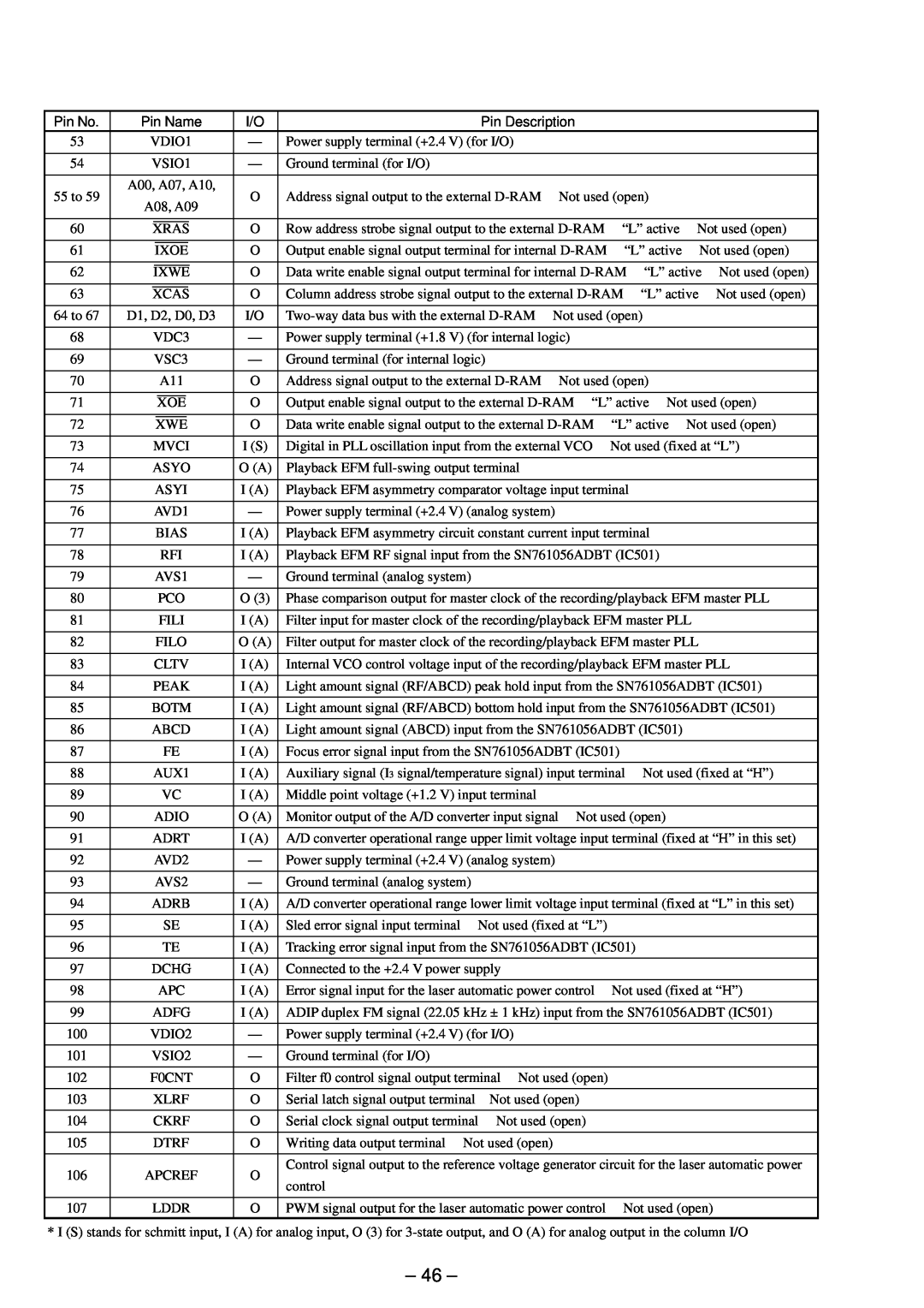
6-9.IC PIN DESCRIPTIONS
MAIN BOARD IC502 CXD2660GA
Page
Page
Page
Page
Page
SECTION EXPLODED VIEWS
Page
SECTION ELECTRICAL PARTS LIST
MAIN
MAIN
MAIN
MAIN
MAIN
Personal Audio Division Company
Sony Corporation
MZ-R70
Published by General Engineering Dept
Ver
US Model Canadian Model AEP Model UK Model
E Model Australian Model Chinese Model
Subject Taiwan model Addition
Top
Page
Image
Contents