14 | The UltraSPARC T2 Processor with CoolThreads Technology | Sun Microsystems, Inc. |
UltraSPARC T2 Processor Architecture
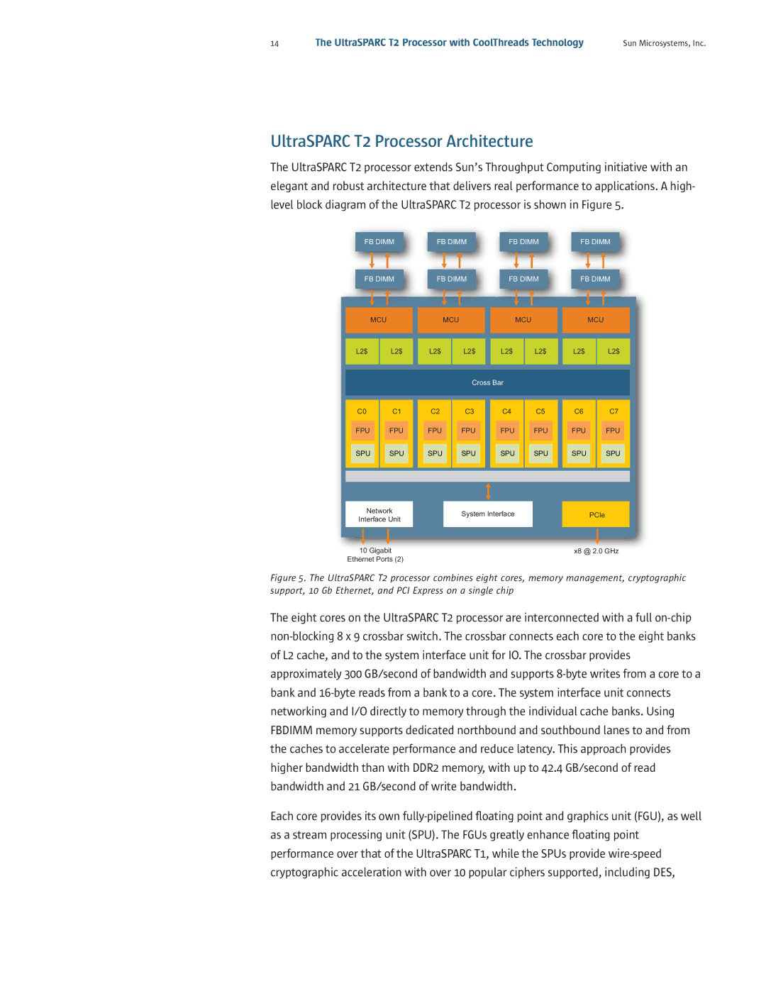
The UltraSPARC T2 processor extends Sun’s Throughput Computing initiative with an elegant and robust architecture that delivers real performance to applications. A high- level block diagram of the UltraSPARC T2 processor is shown in Figure 5.
| | FB DIMM | | | | | FB DIMM | | | | | FB DIMM | | | | | | FB DIMM | |
| | | | | | | | | | | | | | | | | | | | | | | | | | | |
| | | | | | | | | | | | | | | | | | | | | | | | | | | | | | | | | | | | | | |
| | | | | | | | | | | | | | | | | | | | | | | | | | | | | | | | | | | | | | |
| | | | | | | | | | | | | | | | | | | | | | | | | | | | | | | | | | | | | | |
| | FB DIMM | | | | | FB DIMM | | | | | FB DIMM | | | | | | FB DIMM | |
| | | | | | | | | | | | | | | | | | | | | | | | | | | | | | | | | | | | | | |
| | | | | | | | | | | | | | | | | | | | | | | | | | | | | | | | | | | | | | |
| | | | | | | | | | | | | | | | | | | | | | | | | | | | | | | | | | | | | | |
| | | | | | | | | | | | | | | | | | | | | | | | | | | | | | | | | | | | | | |
| | | MCU | | | | | MCU | | | | | MCU | | | | | MCU |
| | | | | | | | | | | | | | | | | | | | | | | | | | | | | | | | | | | | | | |
| | | | | | | | | | | | | | | | | | | | | | | | | | | | | | | | | | | | | | |
| | L2$ | | | | L2$ | | | | L2$ | | | | L2$ | | | | L2$ | | | | L2$ | | | | L2$ | | | | L2$ |
| | | | | | | | | | | | | | | | | | | | | | | | | | | | | | | | | | | | | | |
| | | | | | | | | | | | | | | | | | | | | | | | | | | | | | | | | | | | | |
| | | | | | | | | | | | | | | | Cross Bar | | | | | | | | | | | | | | | | |
| | | | | | | | | | | | | | | | | | | | | | | | | | | | | | | | | | | | | | |
| | | | | | | | | | | | | | | | | | | | | | | | | | | | | | | | | | | | | | |
| | C0 | | | | C1 | | | | C2 | | | | C3 | | | | C4 | | | | C5 | | | | C6 | | | | C7 |
| | | | | | | | | | | | | | | | | | | | | | | | | | | | | | | | | | | | | | |
| FPU | | | | FPU | | | | FPU | | | | FPU | | | | | FPU | | | | FPU | | | | FPU | | | | FPU | |
| | | | | | | | | | | | | | | | | | | | | | | | | | | | | | | | | | | | | | |
| | | | | | | | | | | | | | | | | | | | | | | | | | | | |
| SPU | | | | SPU | | | | SPU | | | | SPU | | | | | SPU | | | | SPU | | | | SPU | | | | SPU | |
| | | | | | | | | | | | | | | | | | | | | | | | | | | | | | | | | | | | | | |
| | | | | | | | | | | | | | | | | | | | | | | | | | | | | | | | | | | | | | |
| | | | | | | | | | | | | | | | | | | | | | | | | | | | | | | | | | | | | | |
| | | | | | | | | | | | | | | | | | | | | | | | | | | | | | | | | | | | | | |
| | | | | | | |
| Network | | System Interface | | PCIe |
Interface Unit | | |
| | | | |
| | | | | |
| | | | | | |
10 Gigabit | | | x8 @ 2.0 GHz |
Ethernet Ports (2) | | | | |
Figure 5. The UltraSPARC T2 processor combines eight cores, memory management, cryptographic support, 10 Gb Ethernet, and PCI Express on a single chip
The eight cores on the UltraSPARC T2 processor are interconnected with a full on-chip non-blocking 8 x 9 crossbar switch. The crossbar connects each core to the eight banks of L2 cache, and to the system interface unit for IO. The crossbar provides approximately 300 GB/second of bandwidth and supports 8-byte writes from a core to a bank and 16-byte reads from a bank to a core. The system interface unit connects networking and I/O directly to memory through the individual cache banks. Using FBDIMM memory supports dedicated northbound and southbound lanes to and from the caches to accelerate performance and reduce latency. This approach provides higher bandwidth than with DDR2 memory, with up to 42.4 GB/second of read bandwidth and 21 GB/second of write bandwidth.
Each core provides its own fully-pipelined floating point and graphics unit (FGU), as well as a stream processing unit (SPU). The FGUs greatly enhance floating point performance over that of the UltraSPARC T1, while the SPUs provide wire-speed cryptographic acceleration with over 10 popular ciphers supported, including DES,