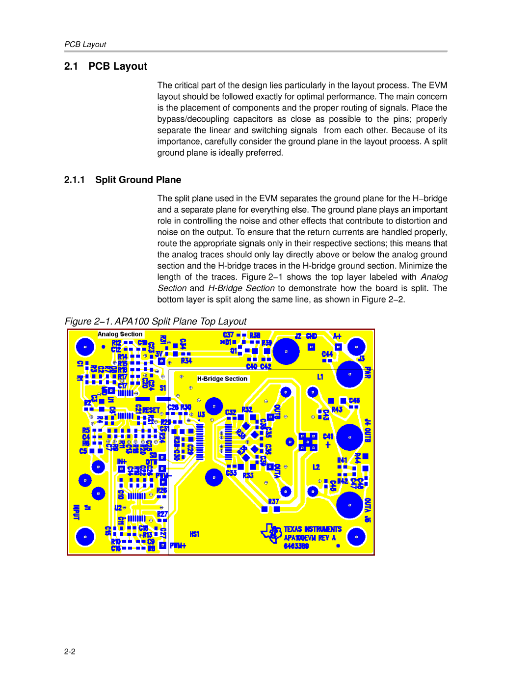
APA100 specifications
Texas Instruments is known for its innovation in the field of analog and embedded processing, with the APA100 being one of its noteworthy products. The APA100 is an advanced analog front-end (AFE) device designed to meet the needs of various applications including industrial, automotive, medical, and consumer electronics.One of the standout features of the APA100 is its high-resolution data conversion capability. It integrates both analog-to-digital converters (ADCs) and digital-to-analog converters (DACs), providing unmatched precision and accuracy in signal processing. The device supports multiple sampling rates, which allows it to adapt to various requirements in different applications, ensuring optimal performance.
The power efficiency of the APA100 is another significant characteristic. Designed with low-power consumption in mind, it enables battery-operated devices to maximize their lifespan while maintaining reliable performance. This energy efficiency makes the APA100 suitable for wearables and portable medical devices, where power management is critical.
In addition to its power efficiency, the APA100 features integrated signal conditioning, which includes amplifiers and filters that enhance the quality of the input signals. This capability reduces the need for external components, thereby simplifying system design and reducing overall costs. With its built-in signal conditioning, engineers can expect improved accuracy and reduced noise in their measurements.
Texas Instruments has also included advanced communication interfaces in the APA100, such as SPI and I2C, to facilitate seamless integration with microcontrollers and processors. This flexibility allows for easy implementation into existing systems, enabling developers to take full advantage of the device's features without extensive re-engineering.
The APA100 is also designed for robustness, featuring a wide operating temperature range, making it suitable for use in harsh environments. This reliability is crucial for industrial applications where device performance can be affected by temperature fluctuations.
Overall, the Texas Instruments APA100 is an exceptional analog front-end device that combines high precision, low power consumption, integrated signal conditioning, and robust design. Its versatile features make it an ideal choice for various applications, paving the way for advancements in technology and improved performance across different sectors. With the APA100, engineers have a powerful tool that can help them innovate and enhance their products in highly competitive markets.

