Additional Sample Schematics
1.6 Additional Sample Schematics
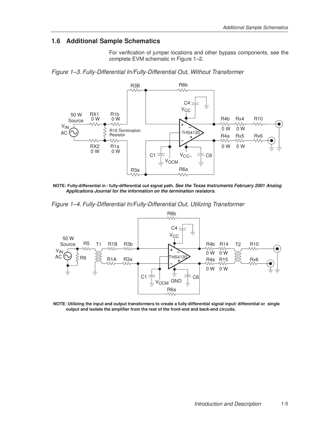
For verification of jumper locations and other bypass components, see the complete EVM schematic in Figure 1±2.
Figure 1±3. Fully-Differential In/Fully-Differential Out, Without Transformer
R3BR6b
50 Ω RX1 | ||
Source | 0 | Ω |
|
| |
VIN
AC
RX2 0 Ω
R1b 0 Ω
R16 Termination Resistor
R1a
0Ω
R3a
| C4 |
|
| VCC |
|
| + |
|
| ± |
|
| THS4130 |
|
| + |
|
| ± |
|
C1 | VCC± | C6 |
| VOCM |
|
R6a
R4b | Rx4 | R10 |
0 Ω | 0 Ω |
|
R4a | Rx5 | Rx6 |
0 Ω | 0 Ω |
|
NOTE:
Figure 1±4. Fully-Differential In/Fully-Differential Out, Utilizing Transformer
|
|
|
|
| R6b |
|
|
|
|
|
|
| C4 |
| |
50 Ω |
|
|
|
| VCC |
| |
R5 |
| R1B | R3b |
|
| R4b | |
Source | T1 | + |
| ||||
VIN |
|
|
|
| ± | 0 Ω | |
|
|
|
|
| |||
AC | R9 |
| R1A | R3a | THS4130 | R4a | |
|
| ± | + | ||||
|
|
|
|
|
| 0 Ω | |
|
|
|
|
|
|
| |
|
|
|
| C1 | VOCM GND | C6 | |
|
|
|
|
|
| ||
|
|
|
|
| R6a |
|
|
R14 T2 R10
0Ω
R15 Rx6
0Ω
NOTE: Utilizing the input and output transformers to create a
Introduction and Description |