Manuals
/
Toshiba
/
Computer Equipment
/
Network Card
Toshiba
TOPAS900
user manual
PCB Routing Top & Bottom View
Models:
TOPAS900
1
42
45
45
Download
45 pages
26.38 Kb
38
39
40
41
42
43
44
45
Board Schematics
Control Switches Reset and NMI
MCU Terminal Connectors
What is
Power Supply
Normal Operation Mode
Page 42
Image 42
Users Manual TOPAS900
Flash
V2.0
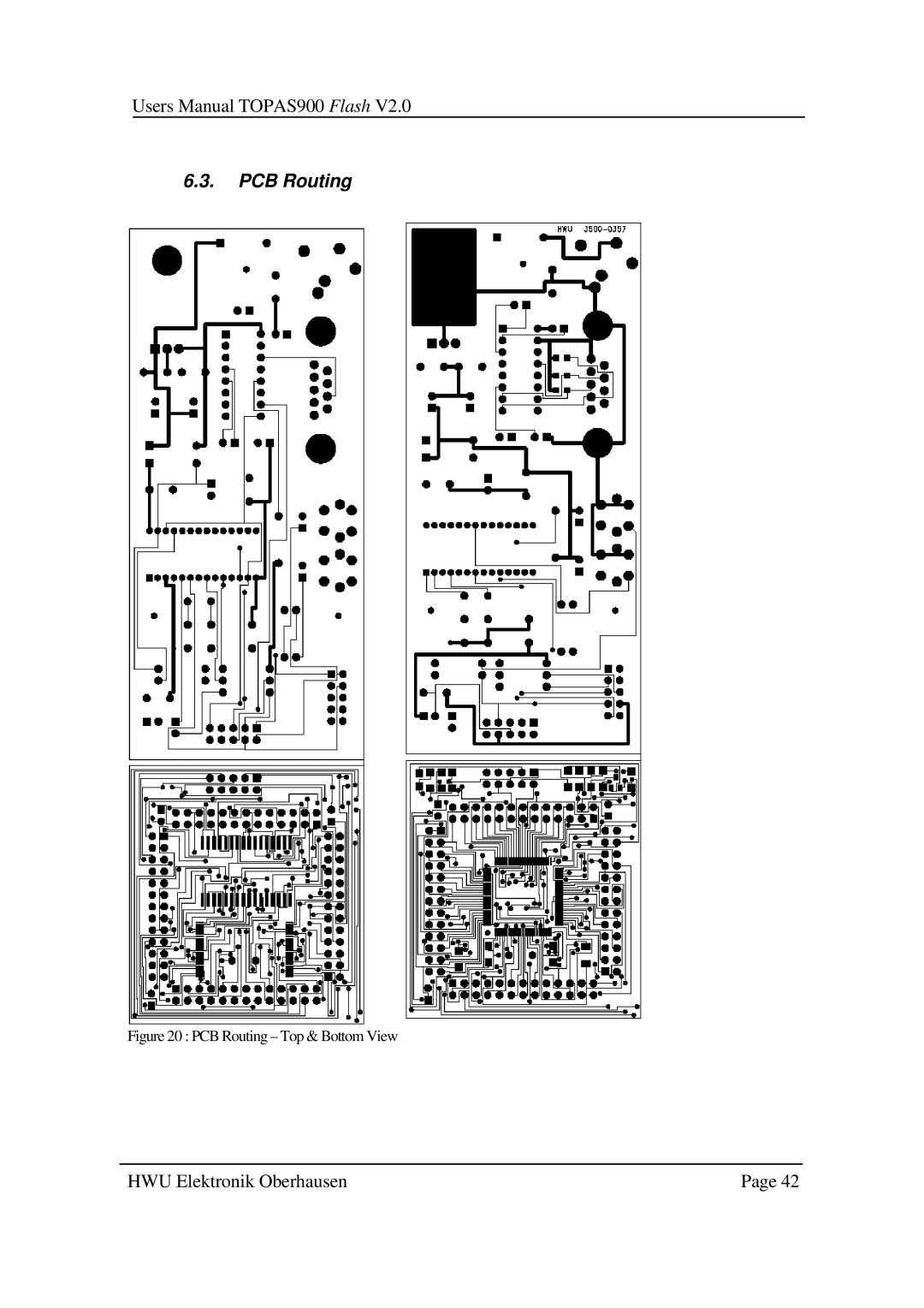
6.3.
PCB Routing
Figure 20 : PCB Routing – Top & Bottom View
HWU Elektronik Oberhausen
Page 42
Page 41
Page 43
Page 42
Image 42
Page 41
Page 43
Contents
TOPAS900 Flash
Preface
Contents
Figures
Definitions and Abbreviations
CPU
What is TOPAS900 Flash?
Key Features of TOPAS900 Flash Package
Introduction
What is in the box?
Let’s start with TOPAS900 Flash
Unpacking
Glance at the TOPAS900 Flash Board
SUB
Principe of Connection
Breaking off TOPAS900 Flash Board from Flash Carrier Board
Programming and Debugging Board
Power Supply
Hardware Description
Firmware Processor
Connector to Flash Carrier Board
Control Switches Reset and NMI
Serial Communication, Connector and Line Driver
Status LEDs
TMP95FY64F Microcontroller
TMP95FY64 Schematic Block Diagram
Kb Flash ROM Toshiba TC58F400 90 ns
Kb RAM Toshiba TC551001 70 ns
Connector to Programming and Debugging Board
MCU Terminal Connectors
Jumpers
Page
Software Description
IAR Tools
Embedded Workbench
Editing Sources
Spy Debugger/Simulator
Spy ROM-Monitor
IAR Tools Limitations
Toshiba Tools
Compiler, Assembler, Linker, Converter
Compile and Link
\SAMPLE\TEST900
TMPro Debugger
TMPro Window
How to create a new debugging profile *.tdp
Page
TMPro ROM-Monitor
Toshiba Tool Limitations
ROM-Monitor Memory Usage
Toshiba ROM-Monitor
F80000H FE0000H
F8C961H
Restrictions of ROM-Monitor Usage
Resource Type IAR C-Spy ROM-Monitor Toshiba TMPro ROM
Functional Description
Operating Modes
MCU Internal Memory Map
Programming in Single Boot Mode
Internal Mapping in different Modes
Normal Operation Mode
Memory MAP
Memory Map for using external / internal Flash
Jumpers of the Flash Carrier Board
Jumper Description
Jumpers of the Programming-Debugging Board
Programming of Flash Memory
Flash Programmer Window
Board Schematics
Technical Sheets
Schematic Page 1
Schematic Page 2
Schematic Page 3
Schematic Page 4
Component Print
Component Print Top & Bottom View
PCB Routing
PCB Routing Top & Bottom View
Application Board
Application Board
∙ TOPAS900 can
Electromagnetic Compatibility
Top
Page
Image
Contents