BOARD LAYOUT GUIDELINES
If you are at all familiar with RF devices, you may be concerned about specialized board layout requirements. Fortunately, because of the care taken by Linx in designing the modules, integrating them is very straightforward. Despite this ease of application, it is still necessary to maintain respect for the RF stage and exercise appropriate care in layout and application in order to maximize performance and ensure reliable operation. The antenna can also be influenced by layout choices. Please review this data guide in its entirety prior to beginning your design. By adhering to good layout principles and observing some basic design rules, you will be on the path to RF success.
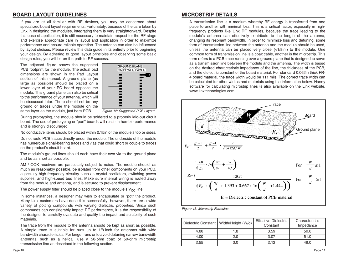
MICROSTRIP DETAILS
A transmission line is a medium whereby RF energy is transferred from one place to another with minimal loss. This is a critical factor, especially in high- frequency products like Linx RF modules, because the trace leading to the module’s antenna can effectively contribute to the length of the antenna, changing its resonant bandwidth. In order to minimize loss and detuning, some form of transmission line between the antenna and the module should be used, unless the antenna can be placed very close (<1/8in.) to the module. One common form of transmission line is a coax cable, another is the microstrip. This term refers to a PCB trace running over a ground plane that is designed to serve as a transmission line between the module and the antenna. The width is based
The adjacent figure shows the suggested PCB footprint for the module. The actual pad dimensions are shown in the Pad Layout section of this manual. A ground plane (as large as possible) should be placed on a lower layer of your PC board opposite the module. This ground plane can also be critical to the performance of your antenna, which will be discussed later. There should not be any ground or traces under the module on the same layer as the module, just bare PCB.
GROUND PLANE
ON LOWER LAYER
Figure 12: Suggested PCB Layout
on the desired characteristic impedance of the line, the thickness of the PCB, and the dielectric constant of the board material. For standard 0.062in thick FR- 4 board material, the trace width would be 111 mils. The correct trace width can be calculated for other widths and materials using the information below. Handy software for calculating microstrip lines is also available on the Linx website, www.linxtechnologies.com.
Trace |
Board |
During prototyping, the module should be soldered to a properly
No conductive items should be placed within 0.15in of the module’s top or sides.
Do not route PCB traces directly under the module. The underside of the module has numerous
The module’s ground lines should each have their own via to the ground plane and be as short as possible.
AM / OOK receivers are particularly subject to noise. The module should, as much as reasonably possible, be isolated from other components on your PCB, especially
The power supply filter should be placed close to the module’s VCC line.
In some instances, a designer may wish to encapsulate or “pot” the product. Many Linx customers have done this successfully; however, there are a wide variety of potting compounds with varying dielectric properties. Since such compounds can considerably impact RF performance, it is the responsibility of the designer to carefully evaluate and qualify the impact and suitability of such materials.
The trace from the module to the antenna should be kept as short as possible. A simple trace is suitable for runs up to
Ground plane |
Figure 13: Microstrip Formulas
Dielectric Constant | Width/Height (W/d) | Effective Dielectric | Characteristic |
|
| Constant | Impedance |
4.80 | 1.8 | 3.59 | 50.0 |
|
|
|
|
4.00 | 2.0 | 3.07 | 51.0 |
2.55 | 3.0 | 2.12 | 48.0 |
|
|
|
|
Page 10 | Page 11 |