ELECTRICAL SPECIFICATIONS
Parameter | Designation | Min. | Typical | Max. | Units | Notes |
POWER SUPPLY |
|
|
|
|
|
|
Operating Voltage | VCC | 2.7 | – | 5.2 | VDC | – |
Supply Current | ICC | – | 1.5 | – | mA | 1,4 |
IPDN | – | 1.0 | – | µA | – | |
TRANSMITTER SECTION |
|
|
|
|
|
|
Transmit Frequency Range: | FC |
|
|
|
|
|
| – | 315 | – | MHz | – | |
| – | 418 | – | MHz | – | |
| – | 433.92 | – | MHz | – | |
Center Frequency Accuracy | – | – | +75 | kHz | – |
ABSOLUTE MAXIMUM RATINGS
Supply Voltage VCC | to | +6.0 | VDC | |
Any Input or Output Pin | to | VCC | VDC | |
Operating Temperature | to | +70 | °C | |
Storage Temperature | to | +85 | °C |
Soldering Temperature+225°C for 10 seconds
*NOTE* Exceeding any of the limits of this section may lead to permanent damage to the device. Furthermore, extended operation at these maximum ratings may reduce the life of this device.
PERFORMANCE DATA
Output Power | PO | +2 | +4 | dBm | 2,3 | |
Harmonic Emissions: | PH |
|
|
|
|
|
| – | – | dBc | – | ||
| – | – | dBc | – | ||
| – | – | dBc | – | ||
|
|
|
|
|
|
|
ANTENNA PORT |
|
|
|
|
|
|
RF Output Impedance | ROUT | – | 50 | – | Ω | 4 |
ENCODER SECTION |
|
|
|
|
|
|
Data Length | – | – | 26 bits 3x | – | – | – |
Average Data Duty Cycle | – | – | 50% | – | – | 4 |
Encoder Oscillator | FENC | – | 70 | – | kHz | 4 |
Data Input: |
|
|
|
|
|
|
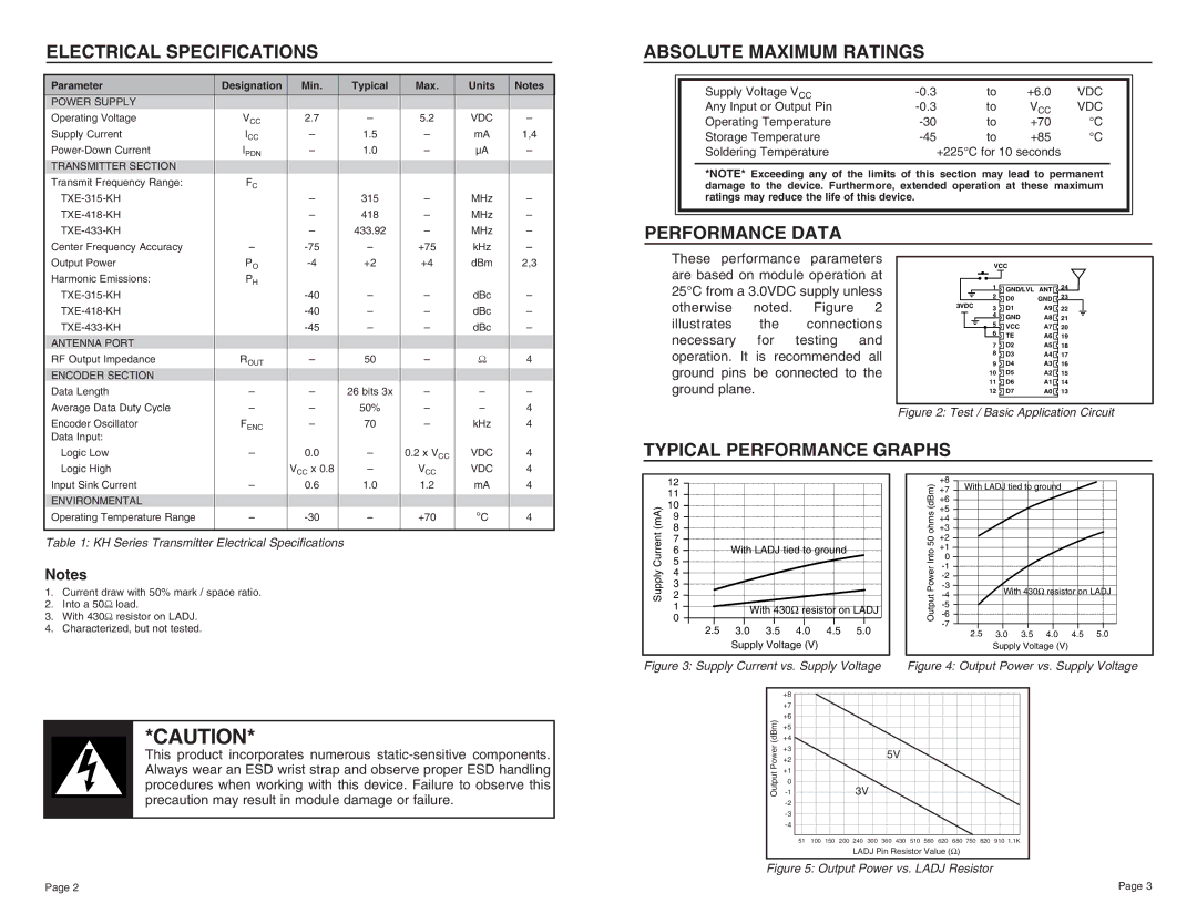
These performance parameters are based on module operation at 25°C from a 3.0VDC supply unless otherwise noted. Figure 2 illustrates the connections necessary for testing and operation. It is recommended all ground pins be connected to the ground plane.
| VCC |
|
| ||
| 1 | GND/LVL | ANT | 24 | |
| 2 | 23 | |||
| D0 | GND | |||
3VDC |
|
| |||
3 | D1 | A9 | 22 | ||
| |||||
| 4 | GND | A8 | 21 | |
| 5 | ||||
| VCC | A7 | 20 | ||
| 6 | ||||
| TE | A6 | 19 | ||
|
| ||||
| 7 | D2 | A5 | 18 | |
| 8 | D3 | A4 | 17 | |
| 9 | D4 | A3 | 16 | |
| 10 | D5 | A2 | 15 | |
| 11 | D6 | A1 | 14 | |
| 12 | D7 | A0 | 13 | |
Figure 2: Test / Basic Application Circuit
Logic Low | – | 0.0 | – | 0.2 x VCC | VDC | 4 |
Logic High |
| VCC x 0.8 | – | VCC | VDC | 4 |
TYPICAL PERFORMANCE GRAPHS
Input Sink Current | – | 0.6 | 1.0 | 1.2 | mA | 4 |
ENVIRONMENTAL |
|
|
|
|
|
|
Operating Temperature Range | – | – | +70 | °C | 4 |
Table 1: KH Series Transmitter Electrical Specifications
Notes
1.Current draw with 50% mark / space ratio.
2.Into a 50Ω load.
3.With 430Ω resistor on LADJ.
4.Characterized, but not tested.
| 12 |
|
|
|
|
|
| 11 |
|
|
|
|
|
(mA) | 10 |
|
|
|
|
|
9 |
|
|
|
|
| |
8 |
|
|
|
|
| |
Current |
|
|
|
|
| |
7 | With LADJ tied to ground |
| ||||
6 |
| |||||
5 |
|
|
|
|
| |
Supply | 4 |
|
|
|
|
|
3 |
|
|
|
|
| |
2 |
|
|
|
|
| |
| 1 | With 430Ω resistor on LADJ | ||||
| 0 |
|
|
|
|
|
| 2.5 | 3.0 | 3.5 | 4.0 | 4.5 | 5.0 |
|
| Supply Voltage (V) |
|
| ||
Figure 3: Supply Current vs. Supply Voltage
(dBm) | +8 |
|
| With LADJ tied to ground | ||||||||||||
+7 |
|
| ||||||||||||||
| +6 |
|
|
|
|
|
|
|
|
|
|
|
|
|
|
|
ohms | +5 |
|
|
|
|
|
|
|
|
|
|
|
|
|
|
|
+3 |
|
|
|
|
|
|
|
|
|
|
|
|
|
|
| |
| +4 |
|
|
|
|
|
|
|
|
|
|
|
|
|
|
|
50 | +2 |
|
|
|
|
|
|
|
|
|
|
|
|
|
|
|
|
|
|
|
|
|
|
|
|
|
|
|
|
| |||
+1 |
|
|
|
|
|
|
|
|
|
|
|
|
|
|
| |
Into |
|
|
|
|
|
|
|
|
|
|
|
|
|
|
| |
0 |
|
|
|
|
|
|
|
|
|
|
|
|
|
|
| |
|
|
|
|
|
|
|
|
|
|
|
|
|
|
|
| |
Power |
|
|
|
|
|
|
|
|
|
|
|
|
|
|
| |
|
|
|
|
|
|
|
|
|
|
|
|
|
|
| ||
|
|
|
|
|
|
|
|
|
|
|
|
|
|
| ||
|
|
|
|
|
|
|
|
|
|
|
|
|
|
|
| |
|
|
|
|
|
|
| With 430Ω resistor on LADJ | |||||||||
|
|
|
|
|
| |||||||||||
Output |
|
|
|
|
|
| ||||||||||
|
|
|
|
|
|
|
|
|
|
|
|
|
|
| ||
|
|
|
|
|
|
|
|
|
|
|
|
|
|
| ||
|
|
|
|
|
|
|
|
|
|
|
|
|
|
|
| |
|
|
|
|
|
|
|
|
|
|
|
|
|
|
|
| |
|
|
|
|
|
|
|
|
|
|
|
|
|
|
|
| |
2.53.0 3.5 4.0 4.5 5.0 Supply Voltage (V)
Figure 4: Output Power vs. Supply Voltage
*CAUTION*
This product incorporates numerous
| +8 |
|
|
|
|
|
|
|
|
|
|
|
|
|
|
| +7 |
|
|
|
|
|
|
|
|
|
|
|
|
|
|
(dBm) | +6 |
|
|
|
|
|
|
|
|
|
|
|
|
|
|
+5 |
|
|
|
|
|
|
|
|
|
|
|
|
|
| |
+4 |
|
|
|
|
|
|
|
|
|
|
|
|
|
| |
Power | +3 |
|
|
|
|
| 5V |
|
|
|
|
|
|
| |
+2 |
|
|
|
|
|
|
|
|
|
|
|
| |||
|
|
|
|
|
|
|
|
|
|
|
|
|
| ||
+1 |
|
|
|
|
|
|
|
|
|
|
|
|
|
| |
Output |
|
|
|
|
|
|
|
|
|
|
|
|
|
| |
0 |
|
|
| 3V |
|
|
|
|
|
|
|
|
| ||
|
|
|
|
|
|
|
|
|
|
|
| ||||
|
|
|
|
|
|
|
|
|
|
|
|
|
|
| |
|
|
|
|
|
|
|
|
|
|
|
|
|
|
| |
|
|
|
|
|
|
|
|
|
|
|
|
|
|
| |
| 51 | 100 | 150 | 200 | 240 | 300 | 360 | 430 | 510 | 560 | 620 | 680 | 750 | 820 | 910 1.1K |
|
|
|
|
| LADJ Pin Resistor Value (Ω) |
|
|
| |||||||
Figure 5: Output Power vs. LADJ Resistor
Page 2 | Page 3 |