
PCA-6187 specifications
The Advantech PCA-6187 is a high-performance industrial PC/104-Plus single-board computer designed to meet the rigorous demands of embedded applications. This robust and versatile board is particularly well-suited for applications in industrial automation, transportation, and telecommunications, where reliability and performance are paramount.One of the main features of the PCA-6187 is its support for the Intel Pentium M and Celeron M processors, providing a potent combination of processing power and energy efficiency. This architecture allows for the execution of complex computation tasks while maintaining a low thermal profile, making it ideal for environments with limited cooling options. Furthermore, the PCA-6187 offers a wide operating temperature range, from -40°C to +85°C, ensuring reliable functionality in extreme conditions.
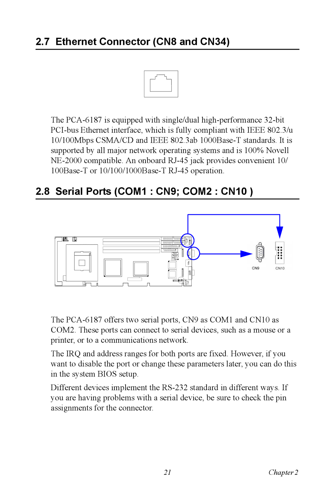
The board incorporates advanced memory capabilities, supporting up to 1GB of SDRAM with a 64-bit data bus. A flash disk interface is also available for high-speed storage solutions, making it easier to manage large amounts of data typical in industrial applications. Additionally, the PCA-6187 features several I/O options, including multiple COM ports, USB interfaces, and parallel ports, allowing for extensive connectivity options for various peripherals and devices.
One of the standout characteristics of the PCA-6187 is its PC/104-Plus form factor, which allows for a modular architecture. This design enables developers to easily expand the capabilities of the board by stacking additional PC/104 modules, facilitating the customization of hardware solutions tailored to specific application requirements. The PCA-6187 also includes watchdog timers to ensure system reliability and prevent system lock-ups, which is critical for mission-critical applications.
Furthermore, the PCA-6187 supports various operating systems, including Windows and Linux, providing developers with flexibility in software development. The integration of rich development resources and tools enhances the speed and efficiency of application deployment in diverse environments.
In conclusion, the Advantech PCA-6187 stands out as a powerful and flexible industrial single-board computer, perfectly suited for a wide array of embedded computing tasks. With its robust design, advanced processing capabilities, and extensive connectivity options, it provides an ideal platform for developers aiming to create reliable systems in demanding operational conditions. The PCA-6187 truly embodies the essence of industrial computing, balancing power and efficiency for a wide range of applications.