The rear-panel TRIGGER connector also provides a trigger output signal. This signal is generated synchronously with the trigger signal sent by the mainframe to the modules. The trigger output signal can be used to trigger an external device such as an oscilloscope, DVM, or another Electronic Load mainframe.

The Electronic Load has a status reporting capability to keep track of trigger operations. Refer to ’Status Reporting’ in the Agilent Electronic Loads Programming Reference Guide.

Slew Rate And Minimum Transition Time

Slew rate is defined as the change in current or voltage over time. A programmable slew rate allows a controlled transition from one load setting to another to minimize induced voltage drops on inductive power wiring, or to control induced transients on a test device (such as would occur during power supply transient response testing).

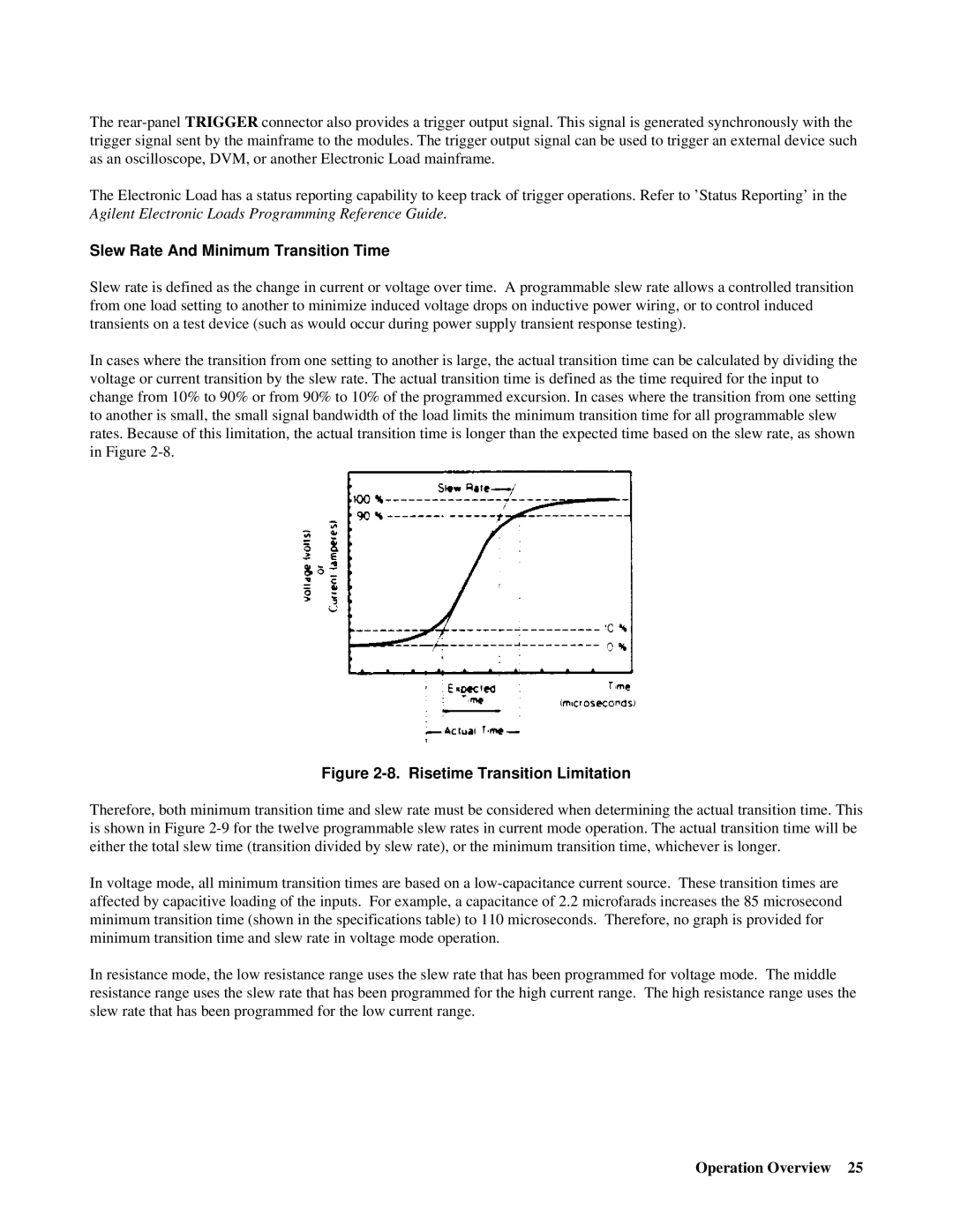
In cases where the transition from one setting to another is large, the actual transition time can be calculated by dividing the voltage or current transition by the slew rate. The actual transition time is defined as the time required for the input to change from 10% to 90% or from 90% to 10% of the programmed excursion. In cases where the transition from one setting to another is small, the small signal bandwidth of the load limits the minimum transition time for all programmable slew rates. Because of this limitation, the actual transition time is longer than the expected time based on the slew rate, as shown in Figure 2-8.

Figure 2-8. Risetime Transition Limitation

Therefore, both minimum transition time and slew rate must be considered when determining the actual transition time. This is shown in Figure 2-9 for the twelve programmable slew rates in current mode operation. The actual transition time will be either the total slew time (transition divided by slew rate), or the minimum transition time, whichever is longer.

In voltage mode, all minimum transition times are based on a low-capacitance current source. These transition times are affected by capacitive loading of the inputs. For example, a capacitance of 2.2 microfarads increases the 85 microsecond minimum transition time (shown in the specifications table) to 110 microseconds. Therefore, no graph is provided for minimum transition time and slew rate in voltage mode operation.

In resistance mode, the low resistance range uses the slew rate that has been programmed for voltage mode. The middle resistance range uses the slew rate that has been programmed for the high current range. The high resistance range uses the slew rate that has been programmed for the low current range.

Operation Overview 25

Page 25
Image 25
Agilent Technologies 6051A, 6050A manual Slew Rate And Minimum Transition Time, Risetime Transition Limitation

6051A, 6050A specifications

Agilent Technologies has long been a leader in providing high-performance test and measurement solutions, and the 6050A and 6051A models exemplify this commitment to quality and innovation. The 6050A and 6051A are versatile signal generators that cater to a diverse range of applications, including research and development, manufacturing, and education, making them essential tools in laboratories and production environments.

The Agilent 6050A is a high-performance RF signal generator known for its frequency range capabilities, which span from 100 kHz to 20 GHz. It offers exceptional phase noise performance and low harmonic distortion, making it ideal for applications that require high signal integrity. The device supports various modulation formats, including AM, FM, and pulse modulation, allowing users to generate a wide range of test signals to simulate real-world conditions.

The 6051A builds upon the robust features of the 6050A with enhanced specifications and additional functionalities. It features a larger frequency modulation bandwidth, pushing the envelope for applications requiring more complex signal generation. The 6051A showcases a superior output power range, ensuring that test signals can be reliably produced at varying power levels. This model also includes advanced output control options that allow for precise signal manipulation, making it particularly suited for testing amplifiers and other RF components.

Both models share core technologies that ensure reliable performance, such as direct digital synthesis (DDS) and phase-locked loop (PLL) architectures. These technologies contribute to the exceptional frequency stability and accuracy that engineers and scientists have come to rely on. Additionally, the user-friendly interface integrated into both models simplifies operation and allows for quick configuration changes, facilitating efficient research and testing workflows.

With comprehensive connectivity options, including GPIB, USB, and Ethernet, the 6050A and 6051A can easily integrate into automated test environments. Their reliability, performance, and flexibility make them a perfect choice for those looking to advance their testing capabilities, whether in academic research, product development, or quality assurance in manufacturing.

In summary, the Agilent Technologies 6050A and 6051A signal generators are powerful tools designed to meet the demands of modern RF testing. Their advanced features, paired with Agilent’s reputation for quality and precision, make them invaluable assets in any engineering or research portfolio. Whether you require sophisticated signal generation for prototype testing or educational purposes, these models will deliver the performance needed to support your objectives.