ADSST-SALEM-3T
PIN CONFIGURATION AND PIN FUNCTION
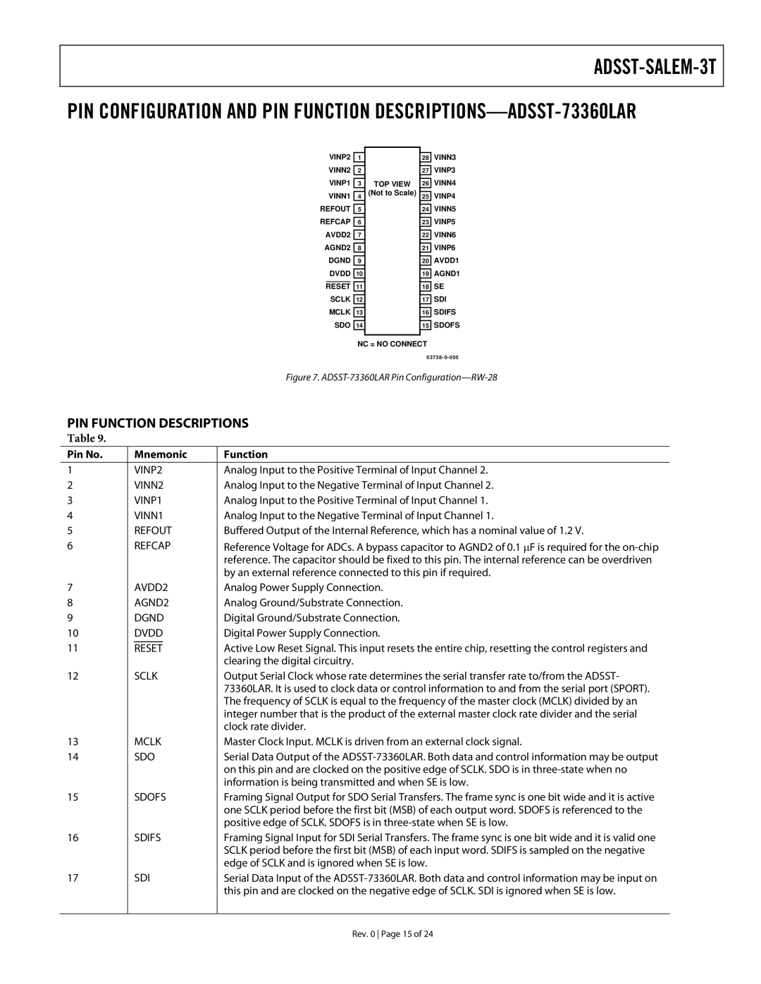
VINP2 1
VINN2 2
VINP1 3
VINN1 4
REFOUT 5 REFCAP 6 AVDD2 7 AGND2 8 DGND 9 DVDD 10 RESET 11
SCLK 12
MCLK 13
SDO 14
TOP VIEW
(Not to Scale)
28VINN3
27VINP3
26VINN4
25VINP4
24VINN5
23VINP5
22VINN6
21VINP6
20AVDD1
19AGND1
18SE
17SDI
16SDIFS
15SDOFS
NC = NO CONNECT
|
|
|
| |
|
|
|
| Figure 7. |
PIN FUNCTION DESCRIPTIONS | ||||
Table 9. |
|
|
|
|
Pin No. |
| Mnemonic | Function | |
|
|
|
|
|
1 |
| VINP2 | Analog Input to the Positive Terminal of Input Channel 2. | |
2 |
| VINN2 | Analog Input to the Negative Terminal of Input Channel 2. | |
3 |
| VINP1 | Analog Input to the Positive Terminal of Input Channel 1. | |
4 |
| VINN1 | Analog Input to the Negative Terminal of Input Channel 1. | |
5 |
| REFOUT | Buffered Output of the Internal Reference, which has a nominal value of 1.2 V. | |
6 |
| REFCAP | Reference Voltage for ADCs. A bypass capacitor to AGND2 of 0.1 ∝F is required for the | |
|
|
|
| reference. The capacitor should be fixed to this pin. The internal reference can be overdriven |
|
|
|
| by an external reference connected to this pin if required. |
7 | AVDD2 | Analog Power Supply Connection. | ||
8 |
| AGND2 | Analog Ground/Substrate Connection. | |
9 |
| DGND | Digital Ground/Substrate Connection. | |
10 | DVDD | Digital Power Supply Connection. | ||
11 |
|
| Active Low Reset Signal. This input resets the entire chip, resetting the control registers and | |
| RESET |
| ||
|
|
|
| clearing the digital circuitry. |
12 |
| SCLK | Output Serial Clock whose rate determines the serial transfer rate to/from the ADSST- | |
|
|
|
| 73360LAR. It is used to clock data or control information to and from the serial port (SPORT). |
|
|
|
| The frequency of SCLK is equal to the frequency of the master clock (MCLK) divided by an |
|
|
|
| integer number that is the product of the external master clock rate divider and the serial |
|
|
|
| clock rate divider. |
13 |
| MCLK | Master Clock Input. MCLK is driven from an external clock signal. | |
14 | SDO | Serial Data Output of the | ||
|
|
|
| on this pin and are clocked on the positive edge of SCLK. SDO is in |
|
|
|
| information is being transmitted and when SE is low. |
15 | SDOFS | Framing Signal Output for SDO Serial Transfers. The frame sync is one bit wide and it is active | ||
|
|
|
| one SCLK period before the first bit (MSB) of each output word. SDOFS is referenced to the |
|
|
|
| positive edge of SCLK. SDOFS is in |
16 |
| SDIFS | Framing Signal Input for SDI Serial Transfers. The frame sync is one bit wide and it is valid one | |
|
|
|
| SCLK period before the first bit (MSB) of each input word. SDIFS is sampled on the negative |
|
|
|
| edge of SCLK and is ignored when SE is low. |
17 |
| SDI | Serial Data Input of the | |
|
|
|
| this pin and are clocked on the negative edge of SCLK. SDI is ignored when SE is low. |
|
|
|
|
|
Rev. 0 Page 15 of 24