ADSST-SALEM-3T
The
VOLTAGE AND CURRENT SENSING
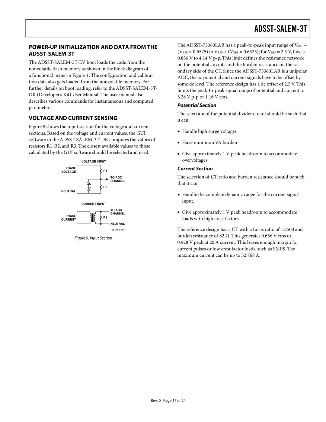
Figure 9 shows the input section for the voltage and current sections. Based on the voltage and current values, the GUI software in the ADSST-SALEM-3T-DK computes the values of resistors R1, R2, and R3. The closest available values to those calculated by the GUI software should be selected and used.
The ADSST-73360LAR has a peak-to-peak input range of VREF – (VREF × 0.6525) to VREF + (VREF × 0.6525); for VREF = 2.5 V, this is 0.856 V to 4.14 V p-p. This limit defines the resistance network on the potential circuits and the burden resistance on the sec- ondary side of the CT. Since the ADSST-73360LAR is a unipolar ADC, the ac potential and current signals have to be offset by some dc level. The reference design has a dc offset of 2.5 V. This limits the peak-to-peak signal range of potential and current to 3.28 V p-p or 1.16 V rms.
Potential Section
The selection of the potential divider circuit should be such that it can:
• Handle high surge voltages | |
• | Have minimum VA burden |
• | Give approximately 1 V peak headroom to accommodate |
VOLTAGE INPUT
PHASE
VOLTAGER1
R2
NEUTRAL
CURRENT INPUT
PHASER3 CURRENT
TO ADC CHANNEL
TO ADC CHANNEL
NEUTRAL
overvoltages. |
Current Section
The selection of CT ratio and burden resistance should be such that it can:
•Handle the complete dynamic range for the current signal input.
•Give approximately 1 V peak headroom to accommodate loads with high crest factors.
The reference design has a CT with a turns ratio of 1:2500 and burden resistance of 82 Ω. This generates 0.656 V rms or
Figure 9. Input Section
0.928 V peak at 20 A current. This leaves enough margin for current pulses or low crest factor loads, such as SMPS. The maximum current can be up to 32.768 A.
Rev. 0 Page 17 of 24