ADSST-SALEM-3T
GENERAL DESCRIPTION OF THE ADSST-218X DSP
The
The DSP combines the
The
The
•Generate the next program address
•Fetch the next instruction
•Perform one or two data moves
•Update one or two data address pointers
•Perform a computational operation
CONTROL
This takes place while the processor continues to:
•Receive and transmit data through the two serial ports
•Receive and/or transmit data through the internal DMA port
•Receive and/or transmit data through the byte DMA port
•Decrement timer
ARCHITECTURE OVERVIEW
The
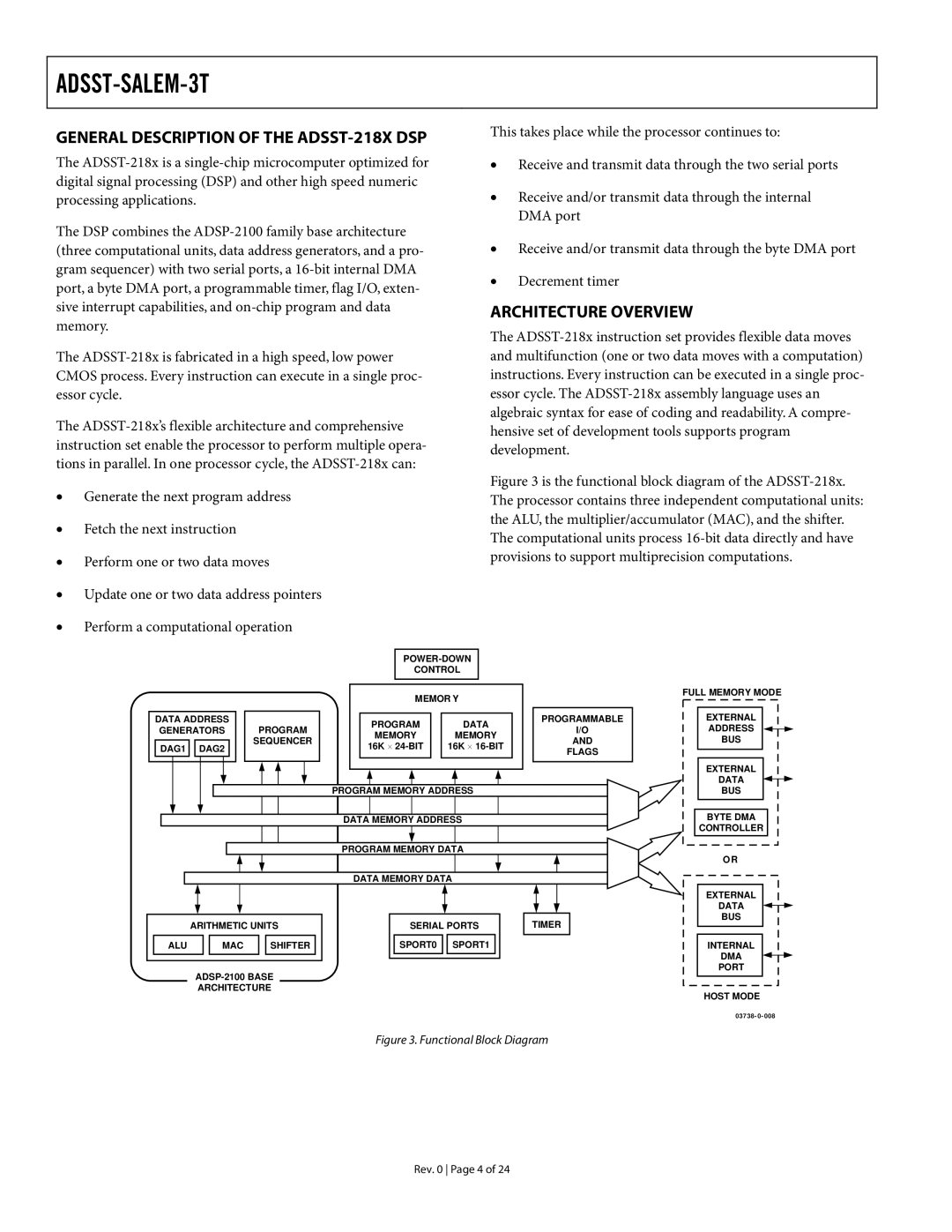
Figure 3 is the functional block diagram of the ADSST-218x. The processor contains three independent computational units: the ALU, the multiplier/accumulator (MAC), and the shifter. The computational units process 16-bit data directly and have provisions to support multiprecision computations.
MEMOR Y
DATA ADDRESS | PROGRAM | PROGRAM | DATA | PROGRAMMABLE | ||
GENERATORS | I/O | |||||
MEMORY | MEMORY | |||||
|
| SEQUENCER | AND | |||
DAG1 | DAG2 | 16K ⋅ | 16K ⋅ | |||
| FLAGS | |||||
|
|
| PROGRAM MEMORY ADDRESS |
| ||
|
|
| DATA MEMORY ADDRESS |
| ||
PROGRAM MEMORY DATA
DATA MEMORY DATA![]()
|
| ARITHMETIC UNITS |
|
| SERIAL PORTS |
| TIMER | ||||||||
|
|
|
|
|
|
|
|
|
|
|
|
|
|
|
|
| ALU |
|
| MAC |
| SHIFTER |
|
|
| SPORT0 |
| SPORT1 |
|
|
|
|
|
|
|
|
|
|
|
|
|
|
|
|
|
|
|
|
|
|
|
|
|
|
|
|
|
|
|
|
|
|
|
|
|
|
|
|
|
|
|
|
| ||||||
|
| ARCHITECTURE |
|
|
|
|
|
|
|
| |||||
Figure 3. Functional Block Diagram
FULL MEMORY MODE
EXTERNAL
ADDRESS
BUS
EXTERNAL
DATA
BUS
BYTE DMA
CONTROLLER
OR
EXTERNAL
DATA
BUS
INTERNAL
DMA
PORT
HOST MODE
03738- 0- 008
Rev. 0 Page 4 of 24