ADSST-SALEM-3T
ADSST-218X ELECTRICAL CHARACTERISTICS
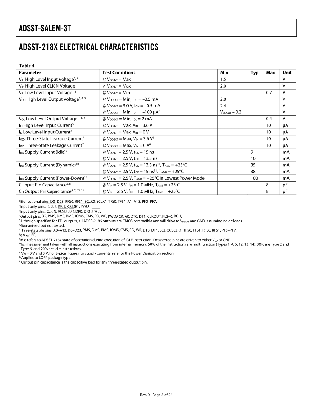
Table 4.
Parameter | Test Conditions | Min | Typ Max | Unit |
|
|
|
|
|
VIH High Level Input Voltage1, 2 | @ VDDINT = Max | 1.5 |
| V |
VIH High Level CLKIN Voltage | @ VDDINT = Max | 2.0 |
| V |
VIL Low Level Input Voltage1, 3 | @ VDDINT = Min |
| 0.7 | V |
VOH High Level Output Voltage1, 4, 5 | @ VDDEXT = Min, IOH = | 2.0 |
| V |
| @ VDDEXT = 3.0 V, IOH = | 2.4 |
| V |
| @ VDDEXT = Min, IOH = | VDDEXT – 0.3 |
| V |
VOL Low Level Output Voltage1, 4, 5 | @ VDDEXT = Min, IOL = 2 mA |
| 0.4 | V |
IIH High Level Input Current3 | @ VDDINT = Max, VIN = 3.6 V |
| 10 | µA |
IIL Low Level Input Current3 | @ VDDINT = Max, VIN = 0 V |
| 10 | µA |
IOZH | @ VDDEXT = Max, VIN = 3.6 V8 |
| 10 | µA |
IOZL | @ VDDEXT = Max, VIN = 0 V8 |
| 10 | µA |
IDD Supply Current (Idle)9 | @ VDDINT = 2.5 V, tCK = 15 ns |
| 9 | mA |
| @ VDDINT = 2.5 V, tCK = 13.3 ns |
| 10 | mA |
IDD Supply Current (Dynamic)10 | @ VDDINT = 2.5 V, tCK = 13.3 ns11, TAMB = +25°C |
| 35 | mA |
| @ VDDINT = 2.5 V, tCK = 15 ns11, TAMB = +25°C |
| 38 | mA |
IDD Supply Current | @ VDDINT = 2.5 V, TAMB = +25°C in Lowest Power Mode |
| 100 | mA |
CI Input Pin Capacitance3, 6 | @ VIN = 2.5 V, fIN = 1.0 MHz, TAMB = +25°C |
| 8 | pF |
CO Output Pin Capacitance6, 7, 12, 13 | @ VIN = 2.5 V, fIN = 1.0 MHz, TAMB = +25°C |
| 8 | pF |
1Bidirectional pins:
2Input only pins: RESET, BR, DR0, DR1, PWD.
3Input only pins: CLKIN, RESET, BR, DR0, DR1, PWD.
4Output pins: BG, PMS, DMS, BMS, IOMS, CMS, RD, WR, PWDACK, A0, DT0, DT1, CLKOUT,
5Although specified for TTL outputs, all
80 V on BR.
9Idle refers to
10IDD measurement taken with all instructions executing from internal memory. 50% of the instructions are multifunction (Types 1, 4, 5, 12, 13, 14), 30% are Type 2 and Type 6, and 20% are idle instructions.
11VIN = 0 V and 3 V. For typical figures for supply currents, refer to the Power Dissipation section.
12Applies to LQFP package type.
13Output pin capacitance is the capacitive load for any
Rev. 0 Page 8 of 24