Analog Devices ADSST-SALEM-3T, ADSST-EM-3040 Grounding and Layout, Ground Plane Layout

Models: ADSST-EM-3040 ADSST-SALEM-3T

1 24
Download 24 pages 13.62 Kb
Page 16
Image 16

ADSST-SALEM-3T

Pin No.

Mnemonic

Function

18

SE

SPORT Enable. Asynchronous input enable pin for the SPORT. When SE is set low by the DSP,


the output pins of the SPORT are three-stated and the input pins are ignored. SCLK is also


disabled internally in order to decrease power dissipation. When SE is brought high, the


control and data registers of the SPORT are at their original values (before SE was brought


low); however, the timing counters and other internal registers are at their reset values.

19

AGND1

Analog Ground Connection.

20

AVDD1

Analog Power Supply Connection.

21

VINP6

Analog Input to the Positive Terminal of Input Channel 6.

22

VINN6

Analog Input to the Negative Terminal of Input Channel 6.

23

VINP5

Analog Input to the Positive Terminal of Input Channel 5.

24

VINN5

Analog Input to the Negative Terminal of Input Channel 5.

25

VINP4

Analog Input to the Positive Terminal of Input Channel 4.

26

VINN4

Analog Input to the Negative Terminal of Input Channel 4.

27

VINP3

Analog Input to the Positive Terminal of Input Channel 3.

28

VINN3

Analog Input to the Negative Terminal of Input Channel 3.


GROUNDING AND LAYOUT

Since the analog inputs to the ADSST-73360LAR are differential, most of the voltages in the analog modulator are common-mode voltages. The excellent common-mode rejection of the part will remove common-mode noise on these inputs. The analog and digital supplies of the ADSST-73360LAR are independent and separately pinned out to minimize coupling between analog and digital sections of the device. The digital filters on the encoder section provide rejection of broadband noise on the power supplies, except at integer multiples of the modulator sampling frequency. The digital filters also remove noise from the analog inputs, provided the source does not saturate the analog modulator. However, because the resolution of the ADSST-73360LAR’s ADC is high and the noise levels from the ADSST-73360LAR are so low, care must be taken with regard to grounding and layout.

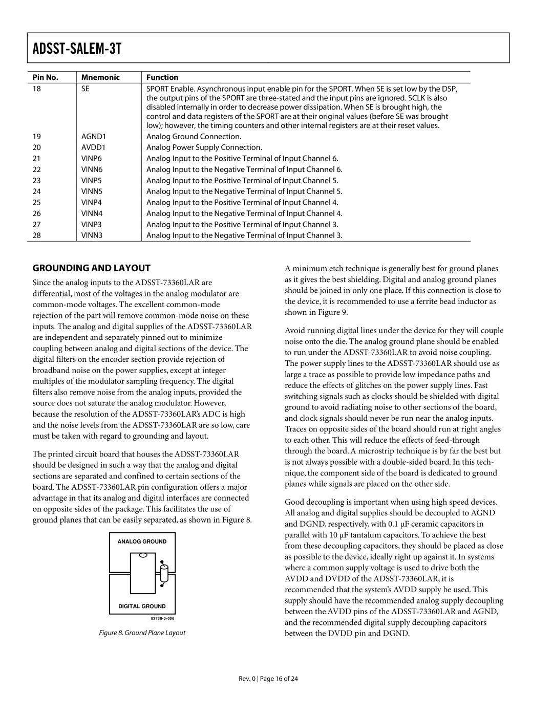
The printed circuit board that houses the ADSST-73360LAR should be designed in such a way that the analog and digital sections are separated and confined to certain sections of the board. The ADSST-73360LAR pin configuration offers a major advantage in that its analog and digital interfaces are connected on opposite sides of the package. This facilitates the use of ground planes that can be easily separated, as shown in Figure 8.

ANALOG GROUND

DIGITAL GROUND

03738-0-006

Figure 8. Ground Plane Layout

A minimum etch technique is generally best for ground planes as it gives the best shielding. Digital and analog ground planes should be joined in only one place. If this connection is close to the device, it is recommended to use a ferrite bead inductor as shown in Figure 9.

Avoid running digital lines under the device for they will couple noise onto the die. The analog ground plane should be enabled to run under the ADSST-73360LAR to avoid noise coupling. The power supply lines to the ADSST-73360LAR should use as large a trace as possible to provide low impedance paths and reduce the effects of glitches on the power supply lines. Fast switching signals such as clocks should be shielded with digital ground to avoid radiating noise to other sections of the board, and clock signals should never be run near the analog inputs. Traces on opposite sides of the board should run at right angles to each other. This will reduce the effects of feed-through through the board. A microstrip technique is by far the best but is not always possible with a double-sided board. In this tech- nique, the component side of the board is dedicated to ground planes while signals are placed on the other side.

Good decoupling is important when using high speed devices. All analog and digital supplies should be decoupled to AGND and DGND, respectively, with 0.1 µF ceramic capacitors in parallel with 10 µF tantalum capacitors. To achieve the best from these decoupling capacitors, they should be placed as close as possible to the device, ideally right up against it. In systems where a common supply voltage is used to drive both the AVDD and DVDD of the ADSST-73360LAR, it is recommended that the system’s AVDD supply be used. This supply should have the recommended analog supply decoupling between the AVDD pins of the ADSST-73360LAR and AGND, and the recommended digital supply decoupling capacitors between the DVDD pin and DGND.

Rev. 0 Page 16 of 24

Page 16
Image 16
Analog Devices ADSST-SALEM-3T, ADSST-EM-3040 specifications Grounding and Layout, Ground Plane Layout