Manuals
/
BIXOLON
/
Computer Equipment
/
Printer
BIXOLON
service manual
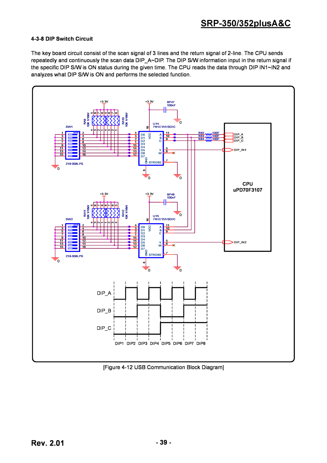
SRP-350/352plusA&C, DIP Switch Circuit
Models:
352plusA
SRP-350
1
39
59
59
Download
59 pages
36.17 Kb
36
37
38
39
40
41
42
43
Troubleshooting
Specification
Install
Wiring Diagram
3-5-1d Signal Description
Maintenance
System Problem
RESET Circuit
SMPS Output Connector
Disassembly and Assembly
Page 39
Image 39
Page 38
Page 40
Page 39
Image 39
Page 38
Page 40
Contents
Service Manual
SRP-350/352plusA&C
Thermal Printer Rev
SRP-350/352plusA&C
Table of Contents
4. Hardware
5. Disassembly and Assembly
6. Adjustments and Maintenance
7. Troubleshooting
1-1 Safety Precautions
1. Precaution Segment
a Remove or reinstall any component or assembly
1-2 Servicing Precaution
1-3 Precaution for Electrostatically Sensitive Devices ESDs
1-4 Operational Precautions
1. Some semiconductor solid state devices are easily damaged by static electricity. Such components are called Electrostatically Sensitive Devices ESDs examples include integrated circuits and some field-effect transistors. The following techniques will reduce the occurrence of component damaged caused by static electricity
2-1-2 Interface Cable Installation
2. Installation and Operation
2-1 Installation
2-1-1 AC Adapter Installation
2-1-5 Wall Mount Installation
SRP-350/352plusA&C
2-2 Operation
2-2-1 Setting the DIP switches
2-2-2 Setting the DIP switch RS-232C Serial Interface
※ Auto Cutter Enable / Disable selection
2-2-3 Setting the DIP switch IEEE1284 Parallel, USB Interface
2-2-5 The self Test Mode
2-2-4 Hexadecimal Dumping
Figure 3-13 The Self-Test Sheet
2-2-6 Setting the Memory Switches
SRP-350/352plusA&C
3-1-2 AC Adapter Dimensions mm
3. Product Specifications
3-1 Appearance
3-1-1 Printer Dimensions mm
3-1-3 Feature Locations-SRP-350/352plusA/C TYPE
SRP-350/352plusCO USB Communication
3-2 General Specifications
SRP-350/352plusCOS RS-232 Serial Communication
SRP-350/352plusCOP IEEE1284 Parallel Communication
Description
3-3 Thermal Printer Specifications
3-3-1 Printer Specification
3-3-2 Character Specification
PD 160R
3-3-3 Paper Specification
3-3-4 Reliability and Environment Specification
※ Note
3-3-5 Printable Area
3-3-6 TPH Thermal Printer Head Specification 1 180dpi
3-3-7 Other Component Specification
3-4 SMPS Specifications
3-4-1 SMPS Switching Mode Power Supply Specification
3-4-2 SMPS Output Connector
3-5 Interface Specifications
3-5-1 RS-232C Serial Interface 3-5-1a Specification
3-5-1b RS-232C I/F Cable
Host
3-5-1d Signal Description
3-5-1c Cable Connection
Printer
※ Note Refer to the Operation Manual about XON/XOFF flow control
2-5-2a Forward Mode Specification Compatibility mode
3-5-1e H/W Flow Control
3-5-1f S/W Flow Control
Busy
3-5-2c Signal Specification Compatibility/Nibble/Byte mode
3-5-2c IEEE1284 I/F Cable
nAck
3-5-3c Cable
3-5-3a Specification
3-5-3b Signal Description
3-5-3 USB2.0 Interface
3-5-4d Construction
From the
Series A Connectors
Series B Connectors
※ Note Minimum conductor construction must be stranded tinned copper
3-6-2 Cable Connection
3-6 Cash Drawer Specifications
※ Note +24V is always output through pin 4 during power on
3-6-1 Drawer Cable
4-1 Wiring Diagram
4. Hardware
Figure 4-1 Board Wiring Diagram
Figure 4-2 Block Diagram
4-2 Block Diagram
VOLTAGE
4-3 Special Circuit Descriptions
4-3-1 Power Circuit
4 CPU, Flesh, SRAM, Reset Voltage +3.3V
ASM811 REUSF-T
4-3-2 RESET Circuit
Reset signal is signal in order to start-up CPU under Power-on
Figure 4-4 Reset Block Diagram Figure 4-5 Reset Waveform
2 Cash Drawer Driving Circuit
4-3-3 Buzzer and Cash Drawer Circuits 1 Buzzer Driving Circuit
4-3-4 I/F PBA Detect Block Diagram
4-3-5 RS-232C Communication Block Diagram
UPD70F3107
4-3-7 USB Communication Block Diagram
4-3-6 Parallel Communication Block Diagram
4-3-8 DIP Switch Circuit
4-3-9 Thermal Printer Head Circuit
DATA#1,2
LATCH
STROBE1
4 Foot Rubber
5. Disassembly and Assembly
5-1 Case lower block
1 Scrw 2 Brkt Dip Switch 3 Case Lower
Screw
8 Screw 1 Screw 2 Brkt PCB
6 Main PCB
5 PCB Serial Parallel
3.Remove the three screws. 4.Separate the Manual cutter from
5-2 Case Upper block
1.Push the button to open the Cove Open. 2.Remove the four screws
1.Remove the two screws
1.Remove the E-Ring. 2.Separate the Spring tension, the
Roller Platen Assembly
1 Spring Hook
4 Brkt-Hook 3 Screw
1 Screw
5-3 Frame block
3 Cover Housing
4 Screw
2 Heatsink Assy 1 Screw
4 Screw 7 Connector
Spring TPH 5.Separate the Connector from the Heat-sink
1.Remove the screw
Slip
1 Screw 2 Frame Main 3 Brkt PCB 4 Power Switch
Frame Main
Washer
6. Adjustments and Maintenance
6-1 Adjustment
6-1-1 Remaining Roll Paper Adjustment
6-1-2 Paper Jam
※ Caution Turn off the printer power before cleaning
6-2 Maintenance
7. Troubleshooting
7-1 Power Problem
Ok? On SMPS
7-2 System Problem
7-3 Panel PBA and Sensor Problem
7-4 Thermal Printer Head and Feed Motor Problem
7-5 Auto Cutter and Drawer Problem
7-6 Dip S/W and I/F PBA Select Problem
Input Ok?
Select Ok?
7-7 RS-232C Serial Communication Problem
7-8 IEEE-1284 Parallel Communication Problem
Reverse Mode
7-9 USB2.0 Communication Problem
Main PBA I/F
Failure?
Top
Page
Image
Contents