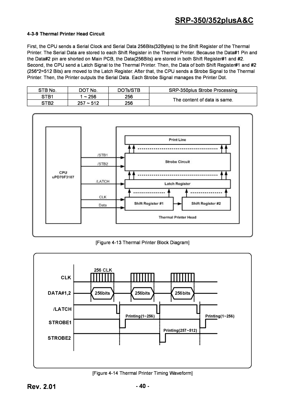
4-3-9 Thermal Printer Head Circuit
First, the CPU sends a Serial Clock and Serial Data 256Bits(32Bytes) to the Shift Register of the Thermal Printer. The Serial Data are stored to each Shift Register in the Thermal Printer. Because the Data#1 Pin and the Data#2 pin are shorted on Main PCB, the Data(256Bits) are stored in both Shift Register#1 and #2. Second, the CPU send a Latch Signal to the Thermal Printer. Then, the Data of both Shift Register#1 and #2 (256*2=512 Bits) are moved to the Latch Register. After that, the CPU sends a Strobe Signal to the Thermal Printer. Then, the Printer outputs the Serial Data. Each Strobe Signal manages the Printer Dot.
STB No. | DOT No. | DOTs/STB | ||
STB1 | 1 ~ 256 | 256 | The content of data is same. | |
STB2 | 257 ~ 512 | 256 | ||
|
| [Figure | ||
| 256 CLK |
|
|
CLK |
|
|
|
DATA#1,2 | 256bits | 256bits | 256bits |
/LATCH |
|
|
|
|
| Printing(1~256) | Printing(1~256) |
STROBE1 |
|
|
|
|
|
| Printing(257~512) |
STROBE2 |
|
|
|
| [Figure | ||
Rev. 2.01 | - 40 - |