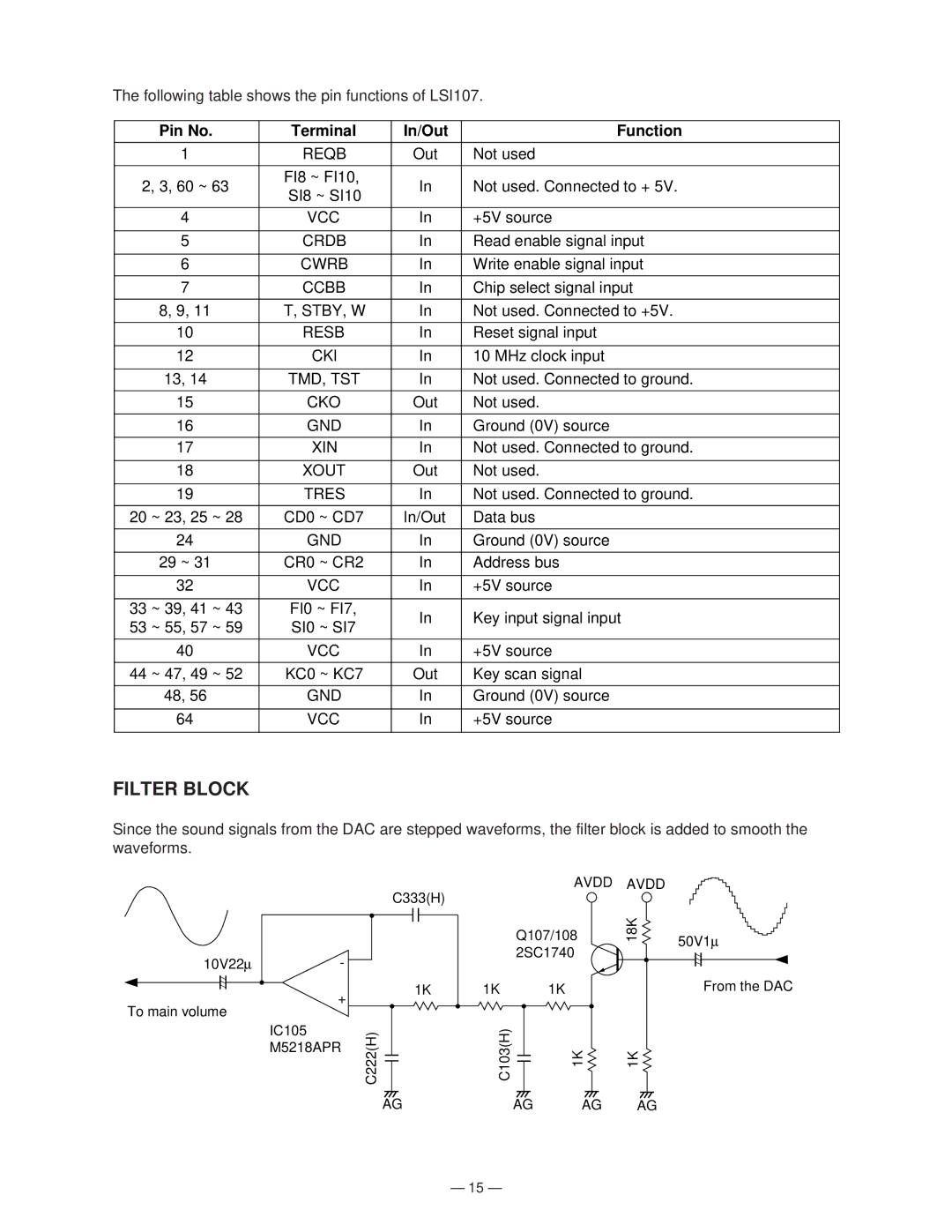
The following table shows the pin functions of LSI107.
Pin No. | Terminal | In/Out | Function | |
|
|
|
| |
1 | REQB | Out | Not used | |
|
|
|
| |
2, 3, 60 ~ 63 | FI8 ~ FI10, | In | Not used. Connected to + 5V. | |
SI8 ~ SI10 | ||||
|
|
| ||
|
|
|
| |
4 | VCC | In | +5V source | |
|
|
|
| |
5 | CRDB | In | Read enable signal input | |
|
|
|
| |
6 | CWRB | In | Write enable signal input | |
|
|
|
| |
7 | CCBB | In | Chip select signal input | |
|
|
|
| |
8, 9, 11 | T, STBY, W | In | Not used. Connected to +5V. | |
|
|
|
| |
10 | RESB | In | Reset signal input | |
|
|
|
| |
12 | CKI | In | 10 MHz clock input | |
|
|
|
| |
13, 14 | TMD, TST | In | Not used. Connected to ground. | |
|
|
|
| |
15 | CKO | Out | Not used. | |
|
|
|
| |
16 | GND | In | Ground (0V) source | |
|
|
|
| |
17 | XIN | In | Not used. Connected to ground. | |
|
|
|
| |
18 | XOUT | Out | Not used. | |
|
|
|
| |
19 | TRES | In | Not used. Connected to ground. | |
|
|
|
| |
20 ~ 23, 25 ~ 28 | CD0 ~ CD7 | In/Out | Data bus | |
|
|
|
| |
24 | GND | In | Ground (0V) source | |
|
|
|
| |
29 ~ 31 | CR0 ~ CR2 | In | Address bus | |
|
|
|
| |
32 | VCC | In | +5V source | |
|
|
|
| |
33 ~ 39, 41 ~ 43 | FI0 ~ FI7, | In | Key input signal input | |
53 ~ 55, 57 ~ 59 | SI0 ~ SI7 | |||
|
| |||
|
|
|
| |
40 | VCC | In | +5V source | |
|
|
|
| |
44 ~ 47, 49 ~ 52 | KC0 ~ KC7 | Out | Key scan signal | |
|
|
|
| |
48, 56 | GND | In | Ground (0V) source | |
|
|
|
| |
64 | VCC | In | +5V source | |
|
|
|
|
FILTER BLOCK
Since the sound signals from the DAC are stepped waveforms, the filter block is added to smooth the waveforms.
10V22∝-
+
To main volume
IC105
M5218APR
C333(H) |
| AVDD | AVDD |
|
|
| |
| Q107/108 | 18K | |
| 2SC1740 |
| |
1K | 1K | 1K |
|
C222(H) | C103(H) | 1K | 1K |
AG | AG | AG | AG |
50V1∝
From the DAC
— 15 —
