|
|
|
| CY25566 | |
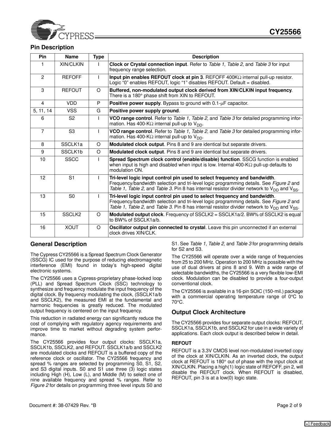
Pin Description |
|
|
|
| |
|
|
|
| ||
Pin | Name | Type | Description | ||
1 | XIN/CLKIN |
| I | Clock or Crystal connection input. Refer to Table 1, Table 2, and Table 3 for input | |
|
|
|
| frequency range selection. | |
2 | REFOFF |
| I | Input pin enables REFOUT clock at pin 3. REFOFF 400KΩ internal | |
|
|
|
| Logic “0” enables REFOUT, logic “1” disables REFOUT. Default = disabled. | |
3 | REFOUT |
| O | Buffered, | |
|
|
|
| There is a 180° phase shift from XIN to REFOUT. | |
4 | VDD |
| P | Positive power supply. Bypass to ground with | |
|
|
|
|
| |
5, 11, 14 | VSS |
| G | Positive power supply ground. | |
|
|
|
|
| |
6 | S2 |
| I | VCO range control. Refer to Table 1, Table 2, and Table 3 for detailed programming infor- | |
|
|
|
| mation. Has | |
7 | S3 |
| I | VCO range control. Refer to Table 1, Table 2, and Table 3 for detailed programming infor- | |
|
|
|
| mation. Has | |
8 | SSCLK1a |
| O | Modulated clock output. Pins 8 and 9 are identical but separate drivers. | |
9 | SSCLK1b |
| O | Modulated clock output. Pins 8 and 9 are identical but separate drivers. | |
|
|
|
|
| |
10 | SSCC |
| I | Spread Spectrum clock control (enable/disable) function. SSCG function is enabled | |
|
|
|
| when input is high and disabled when input is low. Internal | |
|
|
|
| modulation ON. | |
12 | S1 |
| I | ||
|
|
|
| Frequency/bandwidth selection and | |
|
|
|
| Table 1, Table 2, and Table 3. Pin 8 has internal resistor divider network to VDD and VSS. | |
13 | S0 |
| I | ||
|
|
|
| Frequency/bandwidth selection and | |
|
|
|
| Table 1, Table 2, and Table 3. Pin 8 has internal resistor divider network to VDD and VSS. | |
15 | SSCLK2 |
| O | Modulated output clock. Frequency of SSCLK2 = SSCLK1a/2. BW% of SSCLK2 is equal | |
|
|
|
| to BW% of SSCLK1a/b. | |
16 | XOUT |
| O | Oscillator output pin connected to crystal. Leave this pin unconnected if an external | |
|
|
|
| clock drives XIN/CLK. | |
General Description
The Cypress CY25566 is a Spread Spectrum Clock Generator (SSCG) IC used for the purpose of reducing electromagnetic interference (EMI) found in today’s
The CY25566 uses a
This reduction in radiated energy can significantly reduce the cost of complying with regulatory agency requirements and improve time to market without degrading system perfor- mance.
The CY25566 provides four output clocks: SSCLK1a, SSCLK1b, SSCLK2, and REFOUT. SSCLK1a/b and SSCLK2 are modulated clocks and REFOUT is a buffered copy of the reference clock or oscillator. The CY25566 frequency and spread % ranges are selected by programming S0, S1, S2, and S3 digital inputs. S0 and S1 use three (3) logic states including High (H), Low (L), and Middle (M) to select one of nine available frequency and spread % ranges. Refer to Figure 2 for details on programming three level inputs S0 and
S1. See Table 1, Table 2, and Table 3 for programming details for S2 and S3.
The CY25566 will operate over a wide range of frequencies from 25 to 200 MHz. Operation to 200 MHz is possible with the use of dual drivers at pins 8 and 9. With a wide range of selectable bandwidths, the CY25566 is a very flexible
The CY25566 is available in a
Output Clock Architecture
The CY25566 provides four separate output clocks: REFOUT, SSCLK1a, SSCLK1b, and SSCLK2 for use in a wide variety of applications. Each clock output is described below in detail.
REFOUT
REFOUT is a 3.3V CMOS level
Document #: | Page 2 of 9 |
[+] Feedback