CY25566
SSCLK1a/b
SSCLK1a and SSCLK1b are spread spectrum clock outputs used for the purpose of reducing EMI in digital systems. SSCLK1a and SSCLK1b can be connected in several different ways to provide flexibility in application designs. Each clock can drive separate nets with a capacitative load up to 15 pF each or connected together to provide drive to a single net with a capacitative load as high as 33 pF. When both clocks are connected together, the CY25566 is capable of driving 3.3V
Control Logic Structures
The CY25566 has six input control pins for programming VCO range, BW %, Mod ON/OFF and REFOUT ON/OFF. These programmable control pins are described below.
REFOFF
The output clock REFOUT can be enabled or disabled by controlling the state of REFOFF. When REFOFF is at a logic low(0) state, REFOUT is enabled and the reference clock frequency is present at pin 3. When REFOFF is at a logic high state (1), REFOUT is disabled and is set to a logic low state on pin 3. REFOFF has a
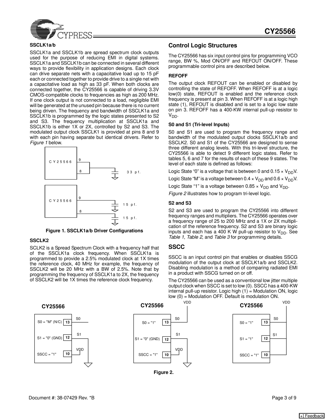
S0 and S1 (Tri-level Inputs)
S0 and S1 are used to program the frequency range and bandwidth of the modulated output clocks SSCLK1a/b and SSCLK2. S0 and S1 of the CY25566 are designed to sense three different analog levels. With this
C Y 2 5 5 6 6
C Y 2 5 5 6 6
9
8
9
8
3 3 p f .
1 5 p f .
1 5 p f .
tables 5, 6 and 7 for the results of each of these 9 states. The level of each state is defined as follows:
Logic State “0” is a voltage that is between 0 and 0.15 × VDDV. Logic State “M” is a voltage between 0.4 × VDD and 0.6 × VDDV. Logic State “1” is a voltage between 0.85 × VDD and VDD.
Figure 2 illustrates how to program tri-level logic.
S2 and S3
S2 and S3 are used to program the CY25566 into different frequency ranges and multipliers. The CY25566 operates over a frequency range of 25 to 200 MHz and a 1X or 2X multipli- cation of the reference frequency. S2 and S3 are binary logic
Figure 1. SSCLK1a/b Driver Configurations
SSCLK2
inputs and each has a 400 K W
SCLK2 is a Spread Spectrum Clock with a frequency half that of the SSCLK1a clock frequency. When SSCLK1a is programmed to provide a 2.5% modulated clock at 1X times the reference clock, 40 MHz for example, the frequency of SSCLK2 will be 20 MHz with a BW of 2.5%. Note that by programming the frequency of SSCLK1a to 2X, the frequency of SSCLK2 will be 1X times the reference clock frequency.
SSCC
SSCC is an input control pin that enables or disables SSCG modulation of the output clock at SSCLK1a/b and SSCLK2. Disabling modulation is a method of comparing radiated EMI in a product with SSCG turned on or off.
The CY25566 can be used as a conventional low jitter multiple output clock when SSCC is set to low (0). SSCC has a
CY25566
S0 = "M" (N/C) |
|
13 | |
|
|
S1 = "0" (GND) | 12 |
|
|
SSCC = "1" | 10 |
|
|
S0
S1
VDD
CY25566
|
|
S0 = "1" | 13 |
|
|
S1 = "0" (GND) | 12 |
|
|
SSCC = "1" | 10 |
|
|
VDD
S0
S1
VDD
CY25566
|
|
S0 = "1" | 13 |
|
|
S1 = "1" | 12 |
|
|
SSCC = "1" | 10 |
|
|
VDD
S0
S1
Figure 2.
Document #: | Page 3 of 9 |
[+] Feedback