CY62128B MoBL®

Maximum Ratings

(Above which the useful life may be impaired. For user guide- lines, not tested.)

Storage Temperature

–65°C to +150°C

Ambient Temperature with


Power Applied

–55°C to +125°C

Supply Voltage on VCC to Relative GND[3] .... –0.5V to +7.0V

DC Voltage Applied to Outputs


in High-Z State[3]

–0.5V to V

+ 0.5V

DC Input Voltage[3]

CC


–0.5V to V

+ 0.5V


CC


Electrical Characteristics Over the Operating Range

Current into Outputs (LOW)

20 mA

Static Discharge Voltage

...........................................

> 2001V

(per MIL-STD-883, Method 3015)


Latch-up Current

> 200 mA

Operating Range


Range


Ambient

V


Temperature (T )[4]

CC


A


Commercial


0°C to +70°C

5V ± 10%


Industrial


–40°C to +85°C

5V ± 10%


Automotive


–40°C to +125°C

5V ± 10%


CY62128B-55

CY62128B-70


Parameter

Description

Test Conditions

Min.

Typ.[2]

Max.

Min.

Typ.[2]

Max.

Unit

VOH

Output HIGH Voltage

VCC = Min., IOH = –1.0 mA

2.4


2.4


V

VOL

Output LOW Voltage

VCC = Min., IOL = 2.1 mA


0.4


0.4

V

VIH

Input HIGH Voltage


2.2


VCC

2.2


VCC

V


+ 0.3


+ 0.3


VIL

Input LOW Voltage[3]


–0.3


0.8

–0.3


0.8

V

IIX

Input Load Current

GND ≤ VI ≤ VCC


–1


+1

–1


+1

µA


Automotive


–10


+10

µA


IOZ

Output Leakage

GND ≤ VI ≤ VCC,


–1


+1

–1


+1

µA


Current

Output Disabled


Automotive


–10


+10

µA


IOS

Output Short Circuit

VCC = Max., VOUT =

GND


–300


–300

mA


Current[5]


ICC

VCC Operating

VCC = Max.,

Industrial,


7.5

20


6

15

mA


Supply Current

IOUT = 0 mA,

Commercial


f = fMAX = 1/tRC


Automotive


6

25

mA

ISB1

Automatic CE

Max. VCC,

Industrial


0.1

2


0.1

1

mA


Power-down Current

CE1 ≥ VIH

Commercial


—TTL Inputs

or CE2 < VIL,


Automotive


0.1

2

mA


VIN ≥ VIH or


VIN ≤ VIL, f = fMAX


ISB2

Automatic CE

Max. VCC,

Industrial


2.5

15


2.5

15

µA


Power-down Current

CE1 ≥ VCC – 0.3V,

Commercial


—CMOS Inputs

or CE2 ≤ 0.3V,


Automotive


2.5

25

µA


VIN ≥ VCC – 0.3V,


or VIN ≤ 0.3V, f = 0


Notes:


3.VIL (min.) = –2.0V for pulse durations of less than 20 ns.

4.TA is the “Instant On” case temperature.

5.Not more than one output should be shorted at one time. Duration of the short circuit should not exceed 30 seconds.

Document #: 38-05300 Rev. *C

Page 3 of 11

[+] Feedback

Page 3
Image 3
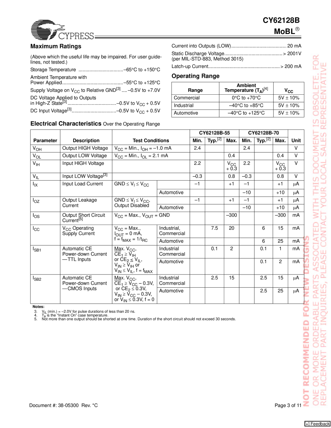
Cypress CY62128B manual Maximum Ratings, Electrical Characteristics Over the Operating Range, Range Ambient Temperature T

CY62128B specifications

The Cypress CY62128B is a high-performance static random-access memory (SRAM) device designed to deliver reliable data storage solutions in a variety of applications. This device is particularly notable for its speed and high-density capabilities, making it suitable for both consumer electronics and industrial applications.

One of the main features of the CY62128B is its organization as a 128K-bit memory chip, which typically comes in a 16K x 8-bit configuration. This allows for efficient processing and storage of data, enabling quick access times. The device boasts access times of 55 ns, making it an excellent choice for applications that require fast data retrieval and processing. Such speed is crucial for modern computing tasks, where delays can significantly impact overall performance.

In addition to its speed, the CY62128B incorporates low-power consumption technology, which is vital for battery-operated devices and other energy-sensitive applications. The operating current is typically in the range of 30 mA, while the standby current is a mere 0.02 mA when the chip is not in use. This combination of low power and high-speed functionality ensures that the device operates efficiently in a wide range of conditions.

The CY62128B also features a wide operating voltage range, accommodating both 2.7V to 5.5V. This versatility allows it to be employed in diverse environments and devices, adapting as necessary to various power supply configurations. Its compatibility with different voltage levels enhances its usability in portable electronics and various embedded systems.

Additionally, the CY62128B benefits from a fast transition between read and write operations, thanks to its asynchronous memory structure. This means that data can be changed and accessed without the need for complex timing sequences, promoting simplicity in system design and reducing overhead.

Another significant characteristic is the robust reliability of the CY62128B, which uses advanced CMOS technology. The chip is built to withstand challenging operating conditions, such as extreme temperatures and radiation exposure, making it suitable for aerospace and military applications.

In summary, the Cypress CY62128B is a versatile and reliable SRAM solution, offering high density, fast access times, low power consumption, and a broad operating voltage range. These features make it an ideal choice for diverse applications, from consumer electronics to industrial systems. Its combination of speed, efficiency, and reliability reflects the innovation that Cypress is known for in the semiconductor industry.