CY62138F MoBL®
AC Test Loads and Waveforms
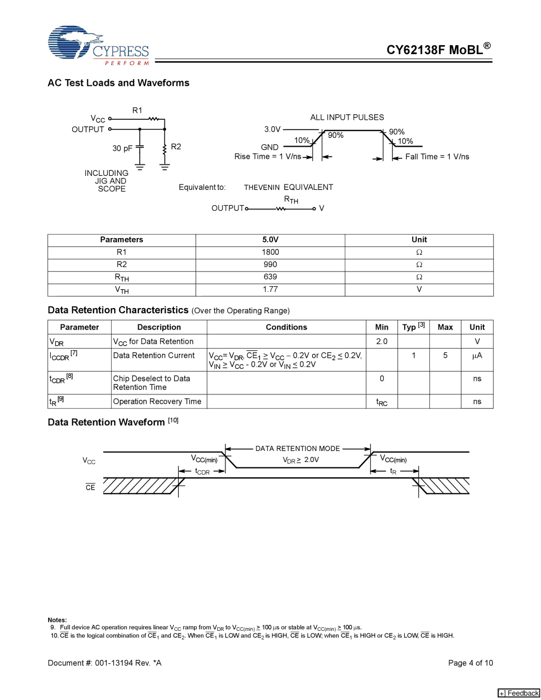
R1
VCC ![]()
ALL INPUT PULSES
OUTPUT ![]()
30 pF ![]()
INCLUDING
JIG AND
SCOPE
|
| 3.0V |
|
|
|
|
|
|
|
| 90% | |||
R2 | 10% |
|
|
|
|
|
| |||||||
|
|
|
|
|
|
| ||||||||
| GND |
|
|
|
|
|
|
|
|
|
| |||
|
|
|
|
|
|
|
|
|
| |||||
| Rise Time = 1 V/ns |
|
|
|
|
|
|
| ||||||
Equivalent to: | THEVENIN EQUIVALENT | |||||||||||||
OUTPUT |
|
|
| RTH |
|
|
|
| V | |||||
|
|
|
|
|
|
| ||||||||
90%
10%
![]() Fall Time = 1 V/ns
Fall Time = 1 V/ns
Parameters | 5.0V | Unit |
R1 | 1800 | Ω |
|
|
|
R2 | 990 | Ω |
|
|
|
RTH | 639 | Ω |
VTH | 1.77 | V |
Data Retention Characteristics (Over the Operating Range)
Parameter | Description |
|
|
| Conditions | Min | Typ [3] | Max | Unit |
VDR | VCC for Data Retention |
|
|
|
| 2.0 |
|
| V |
ICCDR [7] | Data Retention Current | VCC= VDR, |
| 1 | > VCC − 0.2V or CE2 < 0.2V, |
| 1 | 5 | ∝A |
CE | |||||||||
|
| VIN > VCC - 0.2V or VIN < 0.2V |
|
|
|
| |||
tCDR [8] | Chip Deselect to Data |
|
|
|
| 0 |
|
| ns |
| Retention Time |
|
|
|
|
|
|
|
|
tR [9] | Operation Recovery Time |
|
|
|
| tRC |
|
| ns |
Data Retention Waveform [10]
|
| VCC(min) | DATA RETENTION MODE | VCC(min) | |
V | CC | V | > 2.0V | ||
| tCDR | DR |
| tR | |
|
|
|
| ||
CE |
|
|
|
| |
Notes:
9.Full device AC operation requires linear VCC ramp from VDR to VCC(min) > 100 ∝s or stable at VCC(min) > 100 ∝s.
10.CE is the logical combination of CE1 and CE2. When CE1 is LOW and CE2 is HIGH, CE is LOW; when CE1 is HIGH or CE2 is LOW, CE is HIGH.
Document #: | Page 4 of 10 |
[+] Feedback