|
|
|
|
|
|
|
|
|
|
|
| CY62138F MoBL® |
| |
|
|
|
|
|
|
|
|
|
|
|
| |||
|
|
|
|
|
|
|
|
|
|
|
|
|
|
|
|
|
|
|
|
|
|
|
|
|
| ||||
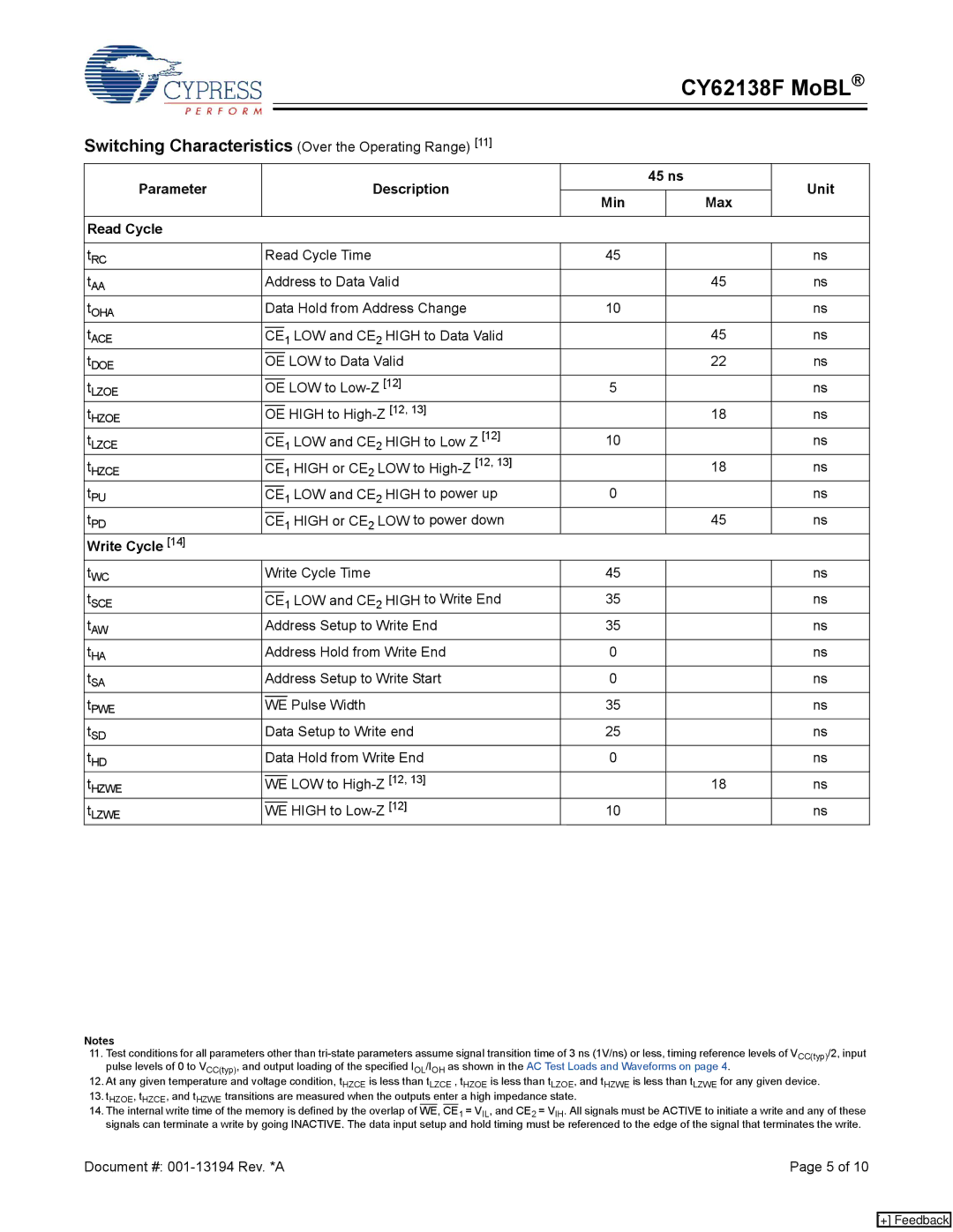
Switching Characteristics (Over the Operating Range) [11] |
|
|
|
|
| |||||||||
| Parameter |
|
|
|
|
|
|
| Description |
| 45 ns | Unit |
| |
|
|
|
|
|
|
|
|
|
|
|
| |||
|
|
|
|
|
|
|
| Min |
| Max |
| |||
|
|
|
|
|
|
|
|
|
|
|
|
| ||
|
|
|
|
|
|
|
|
|
|
|
|
|
| |
Read Cycle |
|
|
|
|
|
|
|
|
|
|
|
| ||
|
|
|
|
|
|
| ||||||||
tRC |
| Read Cycle Time | 45 |
|
| ns |
| |||||||
tAA |
| Address to Data Valid |
|
| 45 | ns |
| |||||||
tOHA |
| Data Hold from Address Change | 10 |
|
| ns |
| |||||||
tACE |
|
|
| 1 LOW and CE2 HIGH to Data Valid |
|
| 45 | ns |
| |||||
CE |
|
| ||||||||||||
tDOE |
|
|
|
|
| LOW to Data Valid |
|
| 22 | ns |
| |||
OE |
|
| ||||||||||||
tLZOE |
|
|
|
|
| LOW to | 5 |
|
| ns |
| |||
OE |
|
|
| |||||||||||
tHZOE |
|
|
|
|
| HIGH to |
|
| 18 | ns |
| |||
OE |
|
| ||||||||||||
tLZCE |
|
|
| 1 LOW and CE2 HIGH to Low Z [12] | 10 |
|
| ns |
| |||||
CE |
|
|
| |||||||||||
t |
|
|
|
|
|
|
| HIGH or CE | LOW to |
|
| 18 | ns |
|
HZCE |
| CE | 1 |
|
| |||||||||
|
|
|
|
| 2 |
|
|
|
|
| ||||
tPU |
|
|
| 1 LOW and CE2 HIGH to power up | 0 |
|
| ns |
| |||||
CE |
|
|
| |||||||||||
tPD |
|
|
| 1 HIGH or CE2 LOW to power down |
|
| 45 | ns |
| |||||
CE |
|
| ||||||||||||
Write Cycle [14] |
|
|
|
|
|
|
|
|
|
|
|
|
| |
tWC |
| Write Cycle Time | 45 |
|
| ns |
| |||||||
tSCE |
|
|
| 1 LOW and CE2 HIGH to Write End | 35 |
|
| ns |
| |||||
CE |
|
|
| |||||||||||
tAW |
| Address Setup to Write End | 35 |
|
| ns |
| |||||||
tHA |
| Address Hold from Write End | 0 |
|
| ns |
| |||||||
tSA |
| Address Setup to Write Start | 0 |
|
| ns |
| |||||||
tPWE |
|
|
|
|
| Pulse Width |
| 35 |
|
| ns |
| ||
WE |
|
|
|
| ||||||||||
tSD |
| Data Setup to Write end | 25 |
|
| ns |
| |||||||
tHD |
| Data Hold from Write End | 0 |
|
| ns |
| |||||||
tHZWE |
|
|
|
|
| LOW to |
|
| 18 | ns |
| |||
WE |
|
| ||||||||||||
tLZWE |
|
|
|
|
| HIGH to | 10 |
|
| ns |
| |||
WE |
|
|
| |||||||||||
Notes
11.Test conditions for all parameters other than
12.At any given temperature and voltage condition, tHZCE is less than tLZCE , tHZOE is less than tLZOE, and tHZWE is less than tLZWE for any given device.
13.tHZOE, tHZCE, and tHZWE transitions are measured when the outputs enter a high impedance state.
14.The internal write time of the memory is defined by the overlap of WE, CE1 = VIL, and CE2 = VIH. All signals must be ACTIVE to initiate a write and any of these signals can terminate a write by going INACTIVE. The data input setup and hold timing must be referenced to the edge of the signal that terminates the write.
Document #: | Page 5 of 10 |
[+] Feedback