CY62148ESL MoBL®
Switching Waveforms
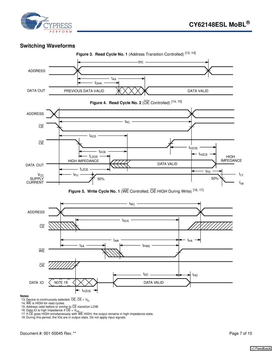
Figure 3. Read Cycle No. 1 (Address Transition Controlled) [13, 14]
tRC
ADDRESS
tAA
tOHA
DATA OUT | PREVIOUS DATA VALID |
|
|
|
| DATA VALID |
|
| |||||
|
|
|
|
|
|
|
| Figure 4. Read Cycle No. 2 (OE Controlled) [14, 15] |
|
|
ADDRESS |
|
|
|
| tRC |
|
|
CE |
|
|
|
| tACE |
|
|
OE |
| tHZOE |
|
| tDOE |
| |
| tHZCE |
| |
| tLZOE | HIGH | |
| HIGH IMPEDANCE |
| IMPEDANCE |
DATA OUT | DATA VALID |
|
|
tLZCE |
|
| |
| tPD |
| |
V | tPU | ICC | |
CC | 50% |
| 50% |
SUPPLY |
| ||
CURRENT |
|
| ISB |
| Figure 5. Write Cycle No. 1 (WE Controlled, OE HIGH During Write) [16, 17] |
| |
|
| tWC |
|
ADDRESS |
|
|
|
|
| tSCE |
|
CE |
|
|
|
| tAW |
| tHA |
| tSA | tPWE |
|
WE |
|
|
|
OE |
|
|
|
|
| tSD | t |
|
|
| HD |
DATA IO | NOTE 18 | DATA VALID |
|
| tHZOE |
|
|
Notes
13.Device is continuously selected. OE, CE = VIL.
14.WE is HIGH for read cycles.
15.Address valid before or similar to CE transition LOW.
16.Data IO is high impedance if OE = VIH.
17.If CE goes HIGH simultaneously with WE HIGH, the output remains in high impedance state.
18.During this period, the IOs are in output state. Do not apply input signals.
Document #: | Page 7 of 10 |
[+] Feedback