CY62256
Electrical Characteristics Over the Operating Range (continued) |
|
|
|
|
|
|
|
|
| |||||||||
|
|
|
|
|
|
|
|
|
|
|
|
|
|
|
|
|
|
|
|
|
|
|
|
|
|
|
|
| CY62256− 55 | CY62256− 70 |
| ||||||
|
|
|
|
|
|
|
|
|
|
|
|
|
|
|
|
| ||
Parameter | Description |
| Test Conditions |
|
| Min. | Typ.[3] |
| Max. | Min. | Typ.[3] | Max. | Unit | |||||
ISB2 | Automatic CE |
|
| Max. VCC, | CE | > VCC − 0.3V |
|
|
| 1 | 5 |
| 1 | 5 | mA | |||
|
| VIN > VCC − | 0.3V, or VIN < |
|
|
|
|
|
|
|
|
|
|
| ||||
|
|
| L |
| 2 | 50 |
| 2 | 50 | ∝ A | ||||||||
| CMOS Inputs |
|
| 0.3V, f = 0 |
|
|
|
|
|
|
|
|
|
|
|
|
|
|
|
|
|
|
|
|
| LL |
| 0.1 | 5 |
| 0.1 | 5 | ∝ A | ||||
|
|
|
|
|
|
|
|
|
|
| ||||||||
|
|
|
|
|
|
|
|
|
|
|
|
|
|
|
|
| ||
|
|
|
| Indust’l Temp Range |
| LL |
| 0.1 | 10 |
| 0.1 | 10 | ∝ A | |||||
|
|
|
|
|
|
|
|
|
|
|
|
|
|
|
|
|
|
|
Capacitance[4] |
|
|
|
|
|
|
|
|
|
|
|
|
|
|
|
|
| |
|
|
|
|
|
|
|
|
|
|
|
|
| ||||||
Parameter |
| Description |
|
|
| Test Conditions |
|
| Max. |
| Unit |
| ||||||
|
|
|
|
|
|
|
|
|
|
|
|
| ||||||
CIN |
| Input Capacitance |
|
| TA = 25° C, f = 1 MHz, |
|
| 6 |
|
| pF |
| ||||||
|
|
|
|
| VCC = 5.0V |
|
|
|
|
|
|
|
|
| ||||
COUT |
| Output Capacitance |
|
|
|
|
|
| 8 |
|
| pF |
| |||||
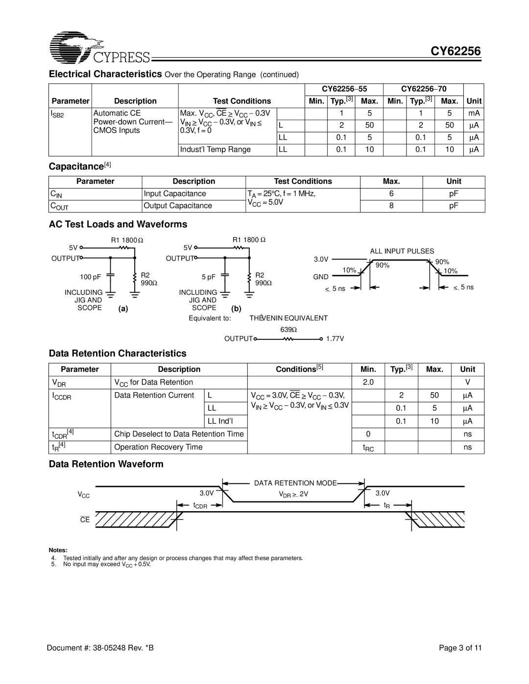
AC Test Loads and Waveforms
R1 1800 Ω | R1 1800 Ω |
5V ![]()
OUTPUT![]()
100 pF
INCLUDING
JIG AND
SCOPE
| 5V |
| OUTPUT |
R2 | 5 pF |
990Ω |
|
INCLUDING JIG AND
(a)SCOPE
| 3.0V |
|
| |
|
|
| ||
R2 | 10% |
| ||
GND |
|
| ||
|
| |||
990Ω |
|
|
|
|
< 5 ns
(b)
ALL INPUT PULSES
90% |
| 90% |
| ||
|
|
10%
< 5 ns
Equivalent to: | THÉVENIN EQUIVALENT |
| 639Ω |
OUTPUT ![]()
![]()
![]()
![]()
![]()
![]()
![]()
![]() 1.77V
1.77V
Data Retention Characteristics
Parameter | Description |
| Conditions[5] | Min. | Typ.[3] | Max. | Unit | ||
VDR | VCC for Data Retention |
|
|
|
| 2.0 |
|
| V |
ICCDR | Data Retention Current | L | VCC = 3.0V, | CE | > VCC − 0.3V, |
| 2 | 50 | ∝ A |
|
|
| VIN > VCC − 0.3V, or VIN < 0.3V |
|
|
|
| ||
|
| LL |
| 0.1 | 5 | ∝ A | |||
|
|
|
|
|
|
|
|
|
|
|
| LL Ind’l |
|
|
|
| 0.1 | 10 | ∝ A |
|
|
|
|
|
|
|
|
|
|
[4] | Chip Deselect to Data Retention Time |
|
|
| 0 |
|
| ns | |
tCDR |
|
|
|
|
| ||||
t [4] | Operation Recovery Time |
|
|
|
| t |
|
| ns |
R |
|
|
|
|
| RC |
|
|
|
Data Retention Waveform
|
| DATA RETENTION MODE |
|
VCC | 3.0V | VDR > 2V | 3.0V |
| tCDR |
| tR |
CE |
|
|
|
Notes:
4.Tested initially and after any design or process changes that may affect these parameters.
5.No input may exceed VCC + 0.5V.
Document #: | Page 3 of 11 |