CY62256
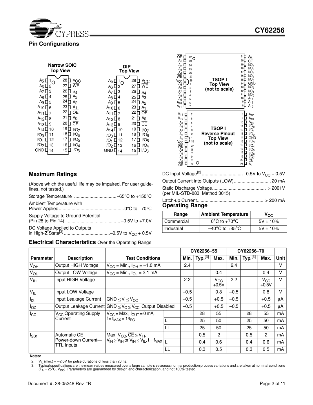
Pin Configurations
Narrow SOIC
Top View
A5 | 1 | 28 | VCC |
A6 | 2 | 27 | WE |
A7 | 3 | 26 | A |
|
|
| 4 |
A8 | 4 | 25 | A3 |
A9 | 5 | 24 | A2 |
A10 | 6 | 23 | A1 |
A11 | 7 | 22 | OE |
A12 | 8 | 21 | A0 |
A13 | 9 | 20 | CE |
A14 | 10 | 19 | I/O |
|
| 18 | 7 |
I/O | 11 | I/O6 | |
0 | 12 | 17 | I/O5 |
I/O | |||
1 |
|
|
|
I/O2 | 13 | 16 | I/O4 |
GND | 14 | 15 | I/O3 |
|
| DIP |
|
| Top View |
| |
A5 | 1 | 28 | VCC |
A6 | 2 | 27 | WE |
A7 | 3 | 26 | A |
|
|
| 4 |
A8 | 4 | 25 | A3 |
A9 | 5 | 24 | A2 |
A10 | 6 | 23 | A1 |
A11 | 7 | 22 | OE |
A12 | 8 | 21 | A0 |
A13 | 9 | 20 | CE |
A14 | 10 | 19 | I/O |
|
| 18 | 7 |
I/O | 11 | I/O6 | |
0 | 12 | 17 | I/O5 |
I/O | |||
1 |
|
|
|
I/O2 | 13 | 16 | I/O4 |
GND | 14 | 15 | I/O3 |
|
|
|
|
|
|
|
|
|
|
|
| A0 | |
| OE |
|
|
| 22 |
| 21 |
| |||||
|
| A1 |
|
|
| 23 |
| 20 |
| CE |
| ||
|
| A2 |
|
|
| 24 |
| 19 |
| I/O7 | |||
|
| A |
|
|
| 25 |
| 18 |
| I/O6 | |||
3 |
|
|
|
|
|
|
|
|
| I/O5 | |||
|
| A4 |
|
|
|
| 26 |
| 17 |
| |||
|
|
|
|
|
|
| |||||||
| WE |
|
|
|
| 27 | TSOP I | 16 |
| I/O4 | |||
V |
|
|
| 28 | 15 |
| I/O3 | ||||||
|
| CC |
|
|
|
| Top View |
|
| GND | |||
|
| A5 |
|
|
| 1 | 14 |
| |||||
|
| A6 |
|
|
| 2 | (not to scale) | 13 |
| I/O2 | |||
|
| A7 |
|
|
| 3 | 12 |
| I/O1 | ||||
|
| A8 |
|
| 4 |
| 11 |
| I/O0 | ||||
|
|
|
|
|
|
|
|
|
|
| A14 | ||
|
| A |
|
|
| 5 |
| 10 |
| ||||
9 |
|
|
|
|
|
|
| 9 |
| A13 | |||
| A |
|
|
| 6 |
|
| ||||||
10 |
|
|
|
|
|
|
|
|
| A12 | |||
| A11 |
|
|
| 7 |
| 8 |
| |||||
|
|
|
|
| |||||||||
|
| A11 |
|
|
|
|
|
|
| A12 | |||
|
|
|
|
| 7 |
| 8 |
| |||||
|
|
|
| ||||||||||
|
| A10 |
|
|
| 6 |
| 9 |
| A13 | |||
|
| A9 |
|
|
| 5 |
| 10 |
| A14 | |||
|
|
|
| ||||||||||
|
| A8 |
|
|
| 4 | TSOP I | 11 |
| I/O0 | |||
|
|
| |||||||||||
|
| A7 |
|
|
| 3 | 12 |
| I/O1 | ||||
|
|
|
|
| Reverse Pinout |
| |||||||
|
| A6 |
|
|
| 2 | 13 |
| I/O2 | ||||
|
|
| |||||||||||
|
| A5 |
|
|
| 1 | Top View | 14 |
| GND | |||
| VCC |
|
|
| 28 | (not to scale) | 15 |
| I/O3 | ||||
|
|
| |||||||||||
|
|
| |||||||||||
|
| WE |
|
|
| 27 | 16 |
| I/O4 | ||||
|
|
|
|
|
|
|
| ||||||
|
| A4 |
|
|
| 26 |
| 17 |
| I/O5 | |||
|
|
|
| ||||||||||
|
| A3 |
|
|
| 25 |
| 18 |
| I/O6 | |||
|
|
|
|
|
|
|
| ||||||
|
| A2 |
|
|
| 24 |
| 19 |
| I/O7 | |||
|
|
|
| ||||||||||
|
| A1 |
|
|
| 23 |
| 20 |
| CE | |||
|
|
|
| ||||||||||
|
| OE |
|
|
|
| 22 |
| 21 |
| A0 | ||
|
|
| |||||||||||
Maximum Ratings
(Above which the useful life may be impaired. For user guide- lines, not tested.)
Storage Temperature | |
Ambient Temperature...................................................with | 0° C to +70° C |
Power Applied | |
Supply Voltage to Ground Potential |
|
(Pin 28 to Pin 14) | |
DC Voltage Applied to Outputs |
|
in |
Electrical Characteristics Over the Operating Range
DC Input Voltage[2] | ................................ | |||
Output Current into Outputs (LOW) |
| 20 mA | ||
Static Discharge Voltage |
| > 2001V | ||
(per |
|
| ||
> 200 mA | ||||
Operating Range |
|
| ||
|
|
|
| |
Range |
| Ambient Temperature | VCC | |
Commercial |
| 0° C to +70° C | 5V ± | 10% |
|
|
|
|
|
Industrial |
| 5V ± | 10% | |
|
|
|
|
|
|
|
|
|
|
| CY62256− 55 | CY62256− 70 |
| ||||
|
|
|
|
|
|
|
|
|
|
| ||
Parameter | Description | Test Conditions |
| Min. | Typ.[3] | Max. | Min. | Typ.[3] | Max. | Unit | ||
VOH | Output HIGH Voltage | VCC = Min., IOH = − 1.0 mA |
| 2.4 |
|
| 2.4 |
|
| V | ||
VOL | Output LOW Voltage | VCC = Min., IOL = 2.1 mA |
|
|
| 0.4 |
|
| 0.4 | V | ||
VIH | Input HIGH Voltage |
|
|
|
| 2.2 |
| VCC | 2.2 |
| VCC | V |
|
|
|
|
|
|
|
| +0.5V |
|
| +0.5V |
|
|
|
|
|
|
|
|
|
|
|
|
|
|
VIL | Input LOW Voltage |
|
|
|
|
| 0.8 |
| 0.8 | V | ||
IIX | Input Leakage Current | GND < VI < VCC |
|
| +0.5 |
| +0.5 | ∝ A | ||||
IOZ | Output Leakage Current | GND < VO < VCC, Output Disabled |
| +0.5 |
| +0.5 | ∝ A | |||||
ICC | VCC Operating Supply | VCC = Max., IOUT = 0 mA, |
|
| 28 | 55 |
| 28 | 55 | mA | ||
| Current | f = fMAX = 1/tRC |
|
|
|
|
|
|
|
| ||
| L |
| 25 | 50 |
| 25 | 50 | mA | ||||
|
|
|
|
| LL |
| 25 | 50 |
| 25 | 50 | mA |
|
|
|
|
|
|
|
|
|
|
| ||
ISB1 | Automatic CE | Max. VCC, | CE | > VIH, |
|
| 0.5 | 2 |
| 0.5 | 2 | mA |
| VIN > VIH or VIN < VIL, f = fMAX |
|
|
|
|
|
|
|
| |||
| L |
| 0.4 | 0.6 |
| 0.4 | 0.6 | mA | ||||
| TTL Inputs |
|
|
|
|
|
|
|
|
|
|
|
|
|
|
| LL |
| 0.3 | 0.5 |
| 0.3 | 0.5 | mA | |
|
|
|
|
|
|
| ||||||
|
|
|
|
|
|
|
|
|
|
|
|
|
Notes:
2.VIL (min.) = − 2.0V for pulse durations of less than 20 ns.
3.Typical specifications are the mean values measured over a large sample size across normal production process variations and are taken at nominal conditions (TA = 25° C, VCC). Parameters are guaranteed by design and characterization, and not 100% tested.
Document #: | Page 2 of 11 |