CY7C09079V/89V/99V

CY7C09179V/89V/99V

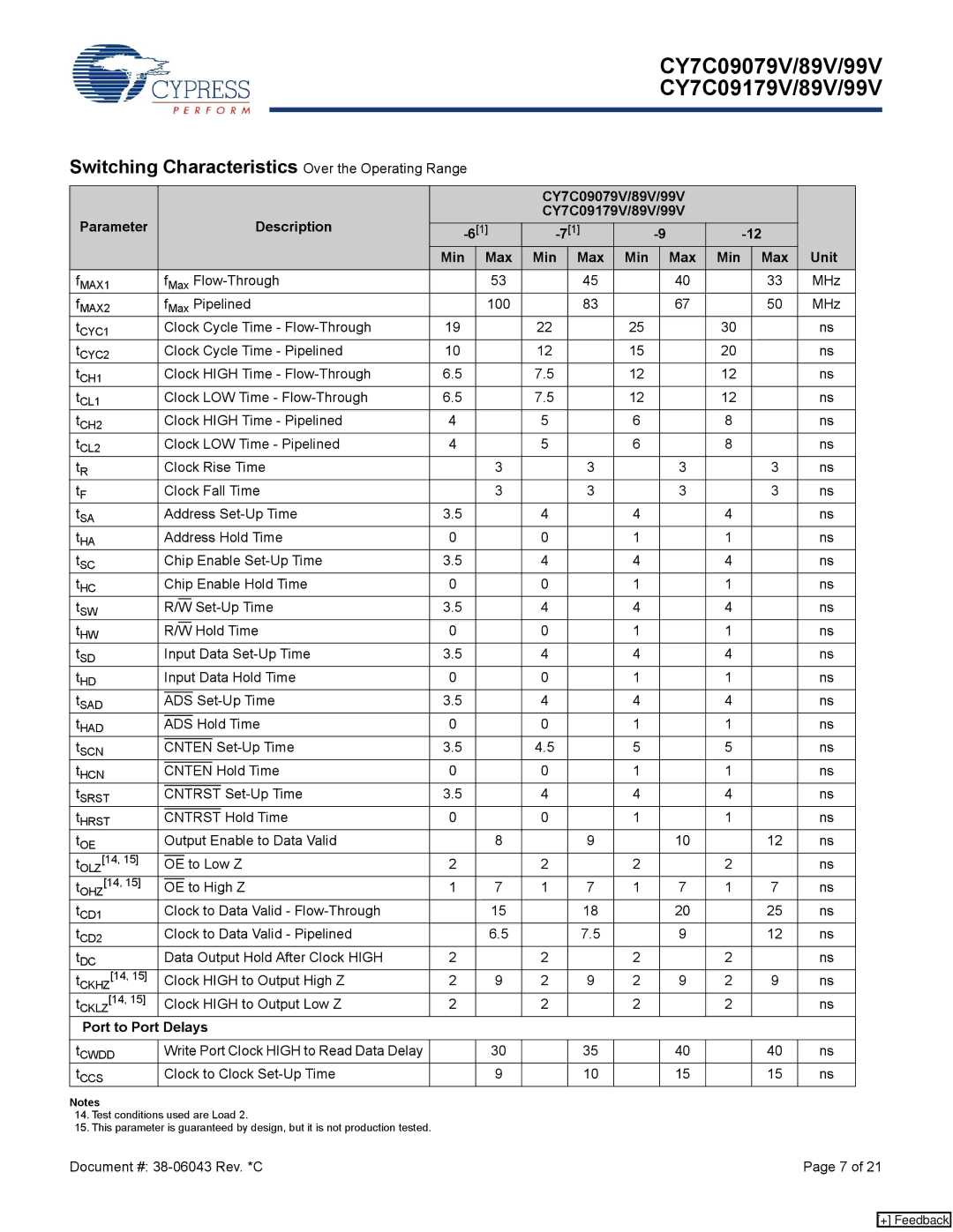
Switching Characteristics Over the Operating Range


CY7C09079V/89V/99V


Parameter


Description


CY7C09179V/89V/99V


-6[1]

-7[1]


-9


-12


Min

Max

Min

Max

Min


Max

Min


Max

Unit

fMAX1


fMax Flow-Through


53


45


40


33

MHz

fMAX2


fMax Pipelined


100


83


67


50

MHz

tCYC1


Clock Cycle Time - Flow-Through

19


22


25


30


ns

tCYC2


Clock Cycle Time - Pipelined

10


12


15


20


ns

tCH1


Clock HIGH Time - Flow-Through

6.5


7.5


12


12


ns

tCL1


Clock LOW Time - Flow-Through

6.5


7.5


12


12


ns

tCH2


Clock HIGH Time - Pipelined

4


5


6


8


ns

tCL2


Clock LOW Time - Pipelined

4


5


6


8


ns

tR


Clock Rise Time


3


3


3


3

ns

tF


Clock Fall Time


3


3


3


3

ns

tSA


Address Set-Up Time

3.5


4


4


4


ns

tHA


Address Hold Time

0


0


1


1


ns

tSC


Chip Enable Set-Up Time

3.5


4


4


4


ns

tHC


Chip Enable Hold Time

0


0


1


1


ns

tSW


R/W


Set-Up Time

3.5


4


4


4


ns

tHW


R/W


Hold Time

0


0


1


1


ns

tSD


Input Data Set-Up Time

3.5


4


4


4


ns

tHD


Input Data Hold Time

0


0


1


1


ns

tSAD


Set-Up Time

3.5


4


4


4


ns

ADS


tHAD


Hold Time

0


0


1


1


ns

ADS


tSCN


Set-Up Time

3.5


4.5


5


5


ns

CNTEN


tHCN


Hold Time

0


0


1


1


ns

CNTEN


tSRST


Set-Up Time

3.5


4


4


4


ns

CNTRST


tHRST


Hold Time

0


0


1


1


ns

CNTRST


tOE


Output Enable to Data Valid


8


9


10


12

ns

tOLZ[14, 15]


to Low Z

2


2


2


2


ns

OE


tOHZ[14, 15]


to High Z

1

7

1

7

1


7

1


7

ns

OE

tCD1


Clock to Data Valid - Flow-Through


15


18


20


25

ns

tCD2


Clock to Data Valid - Pipelined


6.5


7.5


9


12

ns

tDC


Data Output Hold After Clock HIGH

2


2


2


2


ns

tCKHZ[14, 15]


Clock HIGH to Output High Z

2

9

2

9

2


9

2


9

ns

tCKLZ[14, 15]


Clock HIGH to Output Low Z

2


2


2


2


ns

Port to Port Delays


tCWDD


Write Port Clock HIGH to Read Data Delay


30


35


40


40

ns

tCCS


Clock to Clock Set-Up Time


9


10


15


15

ns

Notes

14.Test conditions used are Load 2.

15.This parameter is guaranteed by design, but it is not production tested.

Document #: 38-06043 Rev. *C

Page 7 of 21

[+] Feedback

Page 7
Image 7
Cypress CY7C09099V, CY7C09179V manual Switching Characteristics Over the Operating Range, Ads, Cnten, Port to Port Delays

CY7C09089V, CY7C09189V, CY7C09179V, CY7C09079V, CY7C09199V specifications

Cypress Semiconductor has developed a series of high-performance static random-access memory (SRAM) chips, including the CY7C09099V, CY7C09199V, CY7C09079V, CY7C09179V, and CY7C09189V. These SRAM products are designed for a wide array of applications, ranging from telecommunications and networking to consumer electronics, due to their high speed, low latency, and reliable performance.

One of the most notable features of these CY7C series devices is their high-density configuration. These chips generally offer densities ranging from 256Kb to 16Mb, making them suitable for various applications requiring significant memory capacity without sacrificing speed. Additionally, they typically incorporate a low-power architecture, allowing for efficient energy consumption, which is crucial in battery-operated devices.

The CY7C09099V and CY7C09199V variants are particularly noted for their high-speed access times, achieving data rate performance levels that meet the stringent requirements of modern computing tasks. The read and write access times can vary from 10ns to 15ns, ensuring that these devices can handle fast data processing demands. Their robust performance is complemented by features such as a single supply voltage that simplifies circuit design while providing ease of integration into various systems.

One of the advanced technologies used in these SRAM devices is the asynchronous read and write operation. This technology allows the memory to provide quick data retrieval and storage without the need for complex timing sequences, enhancing overall system responsiveness. Moreover, the chips feature a common data input/output interface, which simplifies communication protocols and reduces design complexity.

Another essential characteristic of the CY7C series is their wide operating temperature range, making them suitable for industrial applications. The ability to operate in diverse environmental conditions increases their reliability across different sectors. Embedded parity checking within the memory architecture helps to detect and correct errors, further ensuring data integrity.

Overall, Cypress’s CY7C09099V, CY7C09199V, CY7C09079V, CY7C09179V, and CY7C09189V SRAM devices represent a significant advancement in memory technology. With a blend of high-speed performance, low power consumption, and robust reliability, they are designed to meet the evolving needs of modern electronic applications, providing designers with a reliable solution for high-performance memory requirements.