CY7C1034DV33
Switching Waveforms (continued)
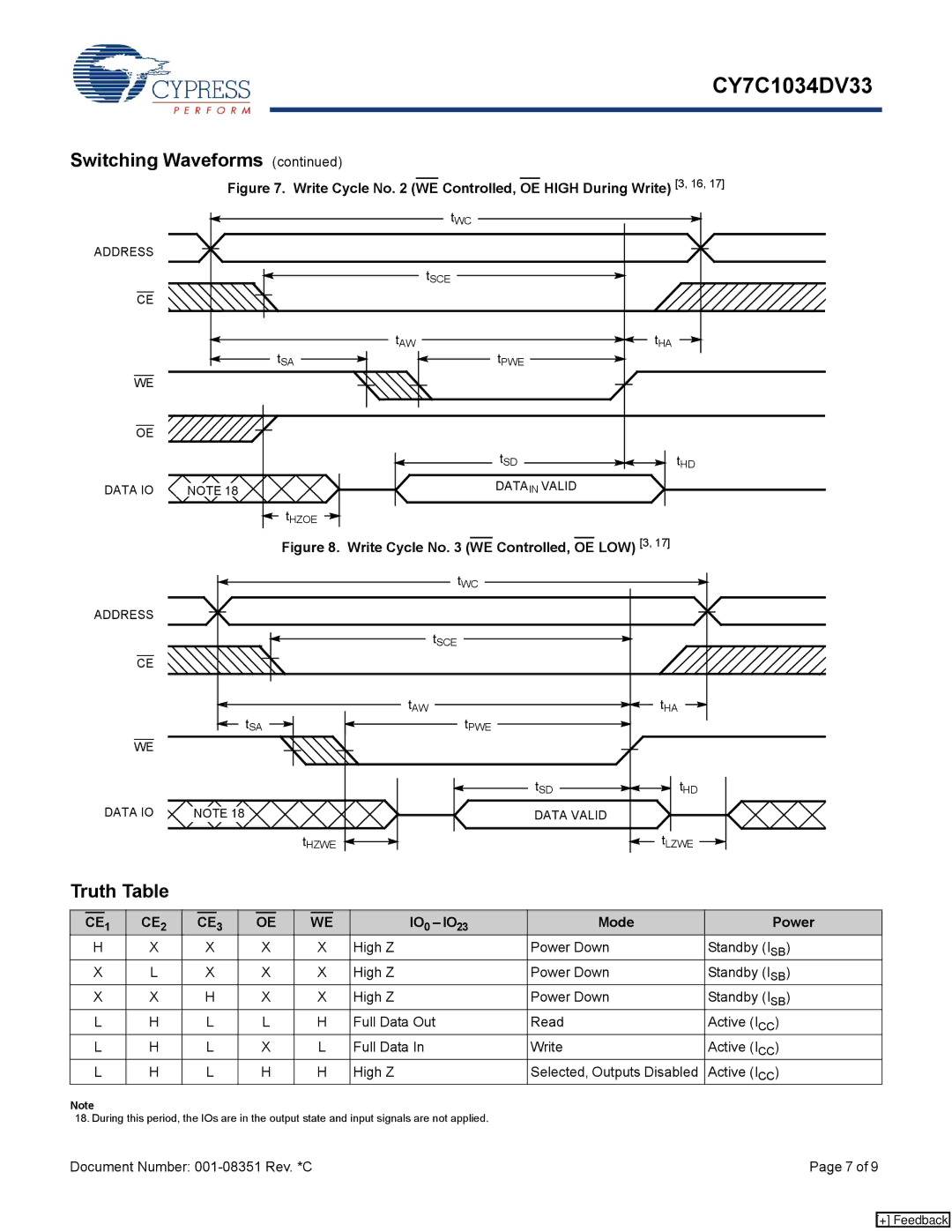
Figure 7. Write Cycle No. 2 (WE Controlled, OE HIGH During Write) [3, 16, 17]
|
| tWC |
|
ADDRESS |
|
|
|
|
| tSCE |
|
CE |
|
|
|
| tAW |
| tHA |
| tSA | tPWE |
|
WE |
|
|
|
OE |
|
|
|
|
| tSD | t |
|
|
| HD |
DATA IO | NOTE 18 | DATAIN VALID |
|
| tHZOE |
|
|
Figure 8. Write Cycle No. 3 (WE Controlled, OE LOW) [3, 17]
|
| tWC |
|
ADDRESS |
|
|
|
|
| tSCE |
|
CE |
|
|
|
| tAW |
| tHA |
| tSA | tPWE |
|
WE |
|
|
|
|
| tSD | tHD |
DATA IO | NOTE 18 | DATA VALID |
|
| tHZWE |
| tLZWE |
Truth Table
CE1 | CE2 | CE3 | OE | WE | IO0 – IO23 | Mode | Power |
H | X | X | X | X | High Z | Power Down | Standby (ISB) |
X | L | X | X | X | High Z | Power Down | Standby (ISB) |
X | X | H | X | X | High Z | Power Down | Standby (ISB) |
L | H | L | L | H | Full Data Out | Read | Active (ICC) |
L | H | L | X | L | Full Data In | Write | Active (ICC) |
L | H | L | H | H | High Z | Selected, Outputs Disabled | Active (ICC) |
Note
18. During this period, the IOs are in the output state and input signals are not applied.
Document Number: | Page 7 of 9 |
[+] Feedback