CY7C1034DV33
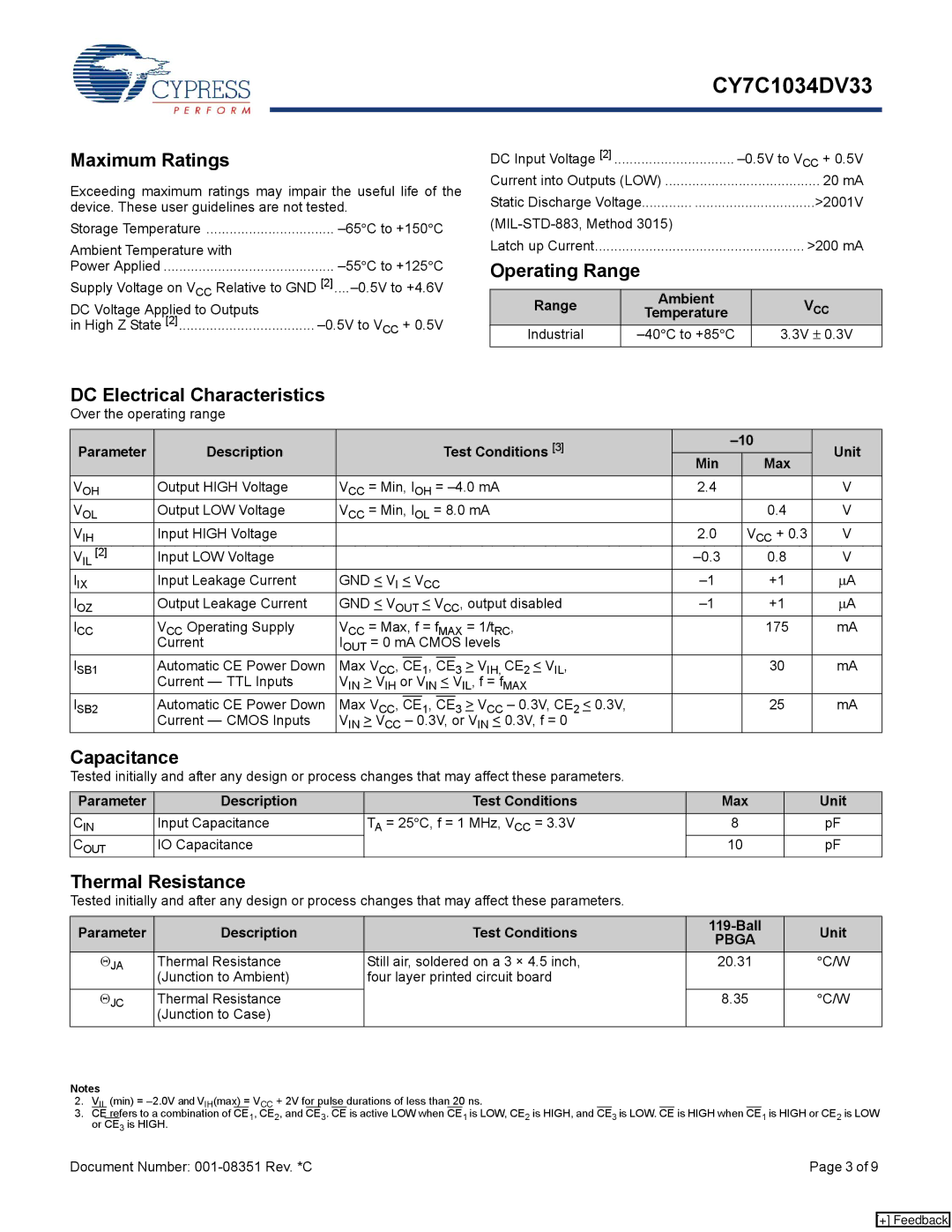
Maximum Ratings
Exceeding maximum ratings may impair the useful life of the device. These user guidelines are not tested.
Storage Temperature | |
Ambient Temperature with |
|
Power Applied |
Supply Voltage on VCC Relative to GND
DC Voltage Applied to Outputs |
|
in High Z State [2] | |
| CC |
DC Input Voltage [2] |
| ||
|
|
| CC |
Current into Outputs (LOW) | 20 mA | ||
Static Discharge Voltage | >2001V | ||
|
| ||
Latch up Current |
|
| >200 mA |
Operating Range |
|
| |
|
|
|
|
Range | Ambient |
| VCC |
Temperature |
| ||
Industrial |
| 3.3V ± 0.3V | |
|
|
|
|
DC Electrical Characteristics
Over the operating range
Parameter | Description |
|
|
| Test Conditions [3] |
| Unit | |||
|
|
| Min |
| Max | |||||
|
|
|
|
|
|
|
|
| ||
VOH | Output HIGH Voltage | VCC = Min, IOH = | 2.4 |
|
| V | ||||
VOL | Output LOW Voltage | VCC = Min, IOL = 8.0 mA |
|
| 0.4 | V | ||||
VIH | Input HIGH Voltage |
|
|
|
|
| 2.0 |
| VCC + 0.3 | V |
VIL [2] | Input LOW Voltage |
|
|
|
|
|
| 0.8 | V | |
IIX | Input Leakage Current | GND < VI < VCC |
| +1 | μA | |||||
IOZ | Output Leakage Current | GND < VOUT < VCC, output disabled |
| +1 | μA | |||||
ICC | VCC Operating Supply | VCC = Max, f = fMAX = 1/tRC, |
|
| 175 | mA | ||||
| Current | IOUT = 0 mA CMOS levels |
|
|
|
| ||||
ISB1 | Automatic CE Power Down | Max VCC, |
| 1, |
| 3 > VIH, CE2 < VIL, |
|
| 30 | mA |
CE | CE |
| ||||||||
| Current — TTL Inputs | VIN > VIH or VIN < VIL, f = fMAX |
|
|
|
| ||||
ISB2 | Automatic CE Power Down | Max VCC, |
| 1, |
| 3 > VCC – 0.3V, CE2 < 0.3V, |
|
| 25 | mA |
CE | CE |
| ||||||||
| Current — CMOS Inputs | VIN > VCC – 0.3V, or VIN < 0.3V, f = 0 |
|
|
|
| ||||
Capacitance
Tested initially and after any design or process changes that may affect these parameters.
Parameter | Description | Test Conditions | Max | Unit |
CIN | Input Capacitance | TA = 25°C, f = 1 MHz, VCC = 3.3V | 8 | pF |
COUT | IO Capacitance |
| 10 | pF |
Thermal Resistance
Tested initially and after any design or process changes that may affect these parameters.
Parameter | Description | Test Conditions | Unit | ||
PBGA | |||||
|
|
|
| ||
ΘJA | Thermal Resistance | Still air, soldered on a 3 × 4.5 inch, | 20.31 | °C/W | |
| (Junction to Ambient) | four layer printed circuit board |
|
| |
ΘJC | Thermal Resistance |
| 8.35 | °C/W | |
| (Junction to Case) |
|
|
|
Notes
2.VIL (min) =
3.CE refers to a combination of CE1, CE2, and CE3. CE is active LOW when CE1 is LOW, CE2 is HIGH, and CE3 is LOW. CE is HIGH when CE1 is HIGH or CE2 is LOW or CE3 is HIGH.
Document Number: | Page 3 of 9 |
[+] Feedback