|
|
|
|
|
| CY7C1034DV33 | ||
|
|
|
|
|
|
|
|
|
|
|
|
|
|
|
|
| |
Ordering Information |
|
|
|
|
| |||
|
|
|
|
|
|
|
| |
Speed | Ordering Code | Package | Package Type |
| Operating | |||
(ns) | Name |
| Range | |||||
|
|
|
|
| ||||
10 | Industrial | |||||||
|
|
|
|
|
|
|
|
|
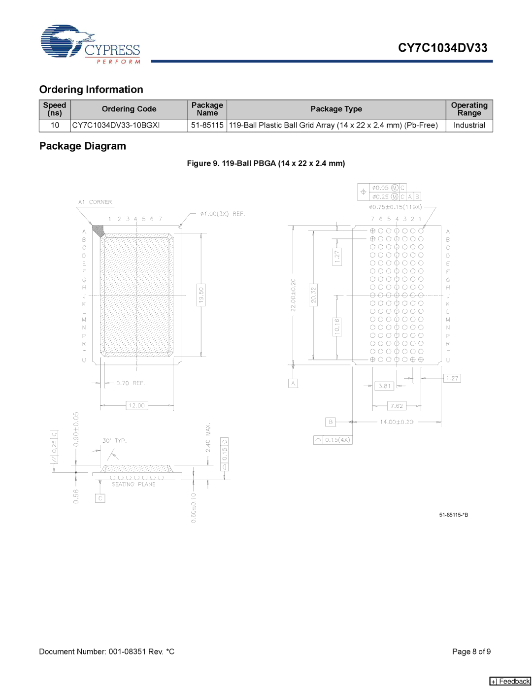
Package Diagram
Figure 9. 119-Ball PBGA (14 x 22 x 2.4 mm)
![]()
Document Number: | Page 8 of 9 |
[+] Feedback