|
|
|
|
|
|
|
|
|
|
|
|
|
|
|
|
|
|
|
|
|
|
| CY7C1223H | ||
|
|
|
|
|
|
|
|
|
|
|
|
|
|
|
|
|
|
|
|
|
|
|
|
|
|
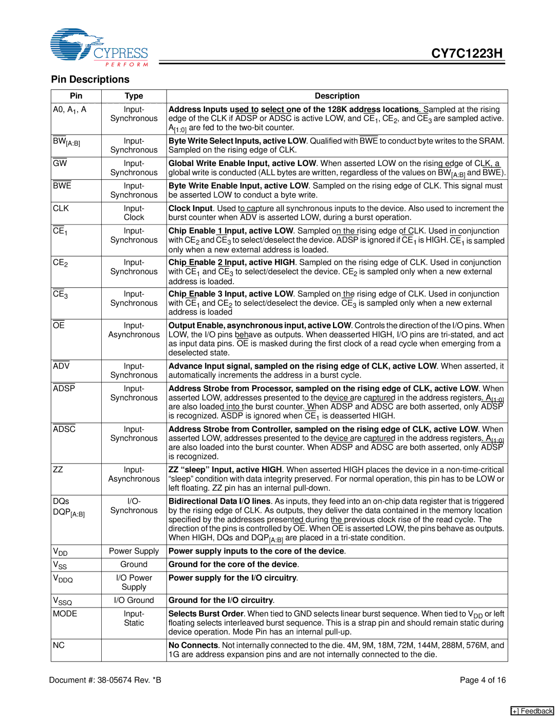
| Pin Descriptions |
|
|
|
|
|
|
|
|
|
|
| |||||||||||||
|
|
|
|
|
|
|
|
|
|
|
|
|
| ||||||||||||
|
|
|
|
|
|
| Pin |
| Type |
|
| Description | |||||||||||||
|
|
|
|
|
|
|
|
| |||||||||||||||||
|
| A0, A1, A |
| Input- | Address Inputs used to select one of the 128K address locations | . | Sampled at the rising | ||||||||||||||||||
|
|
|
|
|
|
|
|
|
|
|
| Synchronous | edge of the CLK if ADSP or ADSC is active LOW, and CE1, CE2, and CE3 are sampled active. | ||||||||||||
|
|
|
|
|
|
|
|
|
|
|
|
|
|
| A[1:0] are fed to the | ||||||||||
|
|
|
|
| [A:B] |
| Input- | Byte Write Select Inputs, active LOW. Qualified with |
| to conduct byte writes to the SRAM. | |||||||||||||||
|
| BW | BWE | ||||||||||||||||||||||
|
|
|
|
|
|
|
|
|
|
|
| Synchronous | Sampled on the rising edge of CLK. | ||||||||||||
|
|
|
|
|
|
|
|
|
|
|
| Input- | Global Write Enable Input, active LOW. When asserted LOW on the rising edge of CLK, a | ||||||||||||
|
| GW | |||||||||||||||||||||||
|
|
|
|
|
|
|
|
|
|
|
| Synchronous | global write is conducted (ALL bytes are written, regardless of the values on BW[A:B] and BWE). | ||||||||||||
|
|
|
|
|
|
|
|
|
|
|
| Input- | Byte Write Enable Input, active LOW. Sampled on the rising edge of CLK. This signal must | ||||||||||||
|
| BWE | |||||||||||||||||||||||
|
|
|
|
|
|
|
|
|
|
|
| Synchronous | be asserted LOW to conduct a byte write. | ||||||||||||
|
| CLK |
| Input- | Clock Input. Used to capture all synchronous inputs to the device. Also used to increment the | ||||||||||||||||||||
|
|
|
|
|
|
|
|
|
|
|
| Clock | burst counter when ADV is asserted LOW, during a burst operation. | ||||||||||||
|
|
| 1 |
|
|
|
| Input- | Chip Enable | 1 | Input, active LOW. Sampled on the rising edge of CLK. Used in conjunction | ||||||||||||||
|
| CE | |||||||||||||||||||||||
|
|
|
|
|
|
|
|
|
|
|
| Synchronous | with CE2 and CE3 to select/deselect the device. ADSP is ignored if CE1 is HIGH. CE1 is sampled | ||||||||||||
|
|
|
|
|
|
|
|
|
|
|
|
|
|
| only when a new external address is loaded. | ||||||||||
|
| CE2 |
| Input- | Chip Enable 2 Input, active HIGH. Sampled on the rising edge of CLK. Used in conjunction | ||||||||||||||||||||
|
|
|
|
|
|
|
|
|
|
|
| Synchronous | with CE1 and CE3 to select/deselect the device. CE2 is sampled only when a new external | ||||||||||||
|
|
|
|
|
|
|
|
|
|
|
|
|
|
| address is loaded. | ||||||||||
|
|
| 3 |
|
|
|
| Input- | Chip Enable 3 Input, active LOW. Sampled on | the | rising edge of CLK. Used in conjunction | ||||||||||||||
|
| CE | |||||||||||||||||||||||
|
|
|
|
|
|
|
|
|
|
|
| Synchronous | with CE1 and CE2 to select/deselect the device. CE3 is sampled only when a new external | ||||||||||||
|
|
|
|
|
|
|
|
|
|
|
|
|
|
| address is loaded | ||||||||||
|
|
|
|
|
|
|
|
| Input- | Output Enable, asynchronous input, active LOW. Controls the direction of the I/O pins. When | |||||||||||||||
|
| OE | |||||||||||||||||||||||
|
|
|
|
|
|
|
|
|
|
|
| Asynchronous | LOW, the I/O pins behave as outputs. When deasserted HIGH, I/O pins are | ||||||||||||
|
|
|
|
|
|
|
|
|
|
|
|
|
|
| as input data pins. OE is masked during the first clock of a read cycle when emerging from a | ||||||||||
|
|
|
|
|
|
|
|
|
|
|
|
|
|
| deselected state. | ||||||||||
|
|
|
|
|
|
|
|
|
|
| Input- | Advance Input signal, sampled on the rising edge of CLK, active LOW. When asserted, it | |||||||||||||
|
| ADV | |||||||||||||||||||||||
|
|
|
|
|
|
|
|
|
|
|
| Synchronous | automatically increments the address in a burst cycle. | ||||||||||||
|
|
|
|
|
|
|
|
|
|
|
| Input- | Address Strobe from Processor, sampled on the rising edge of CLK, active LOW. When | ||||||||||||
|
| ADSP | |||||||||||||||||||||||
|
|
|
|
|
|
|
|
|
|
|
| Synchronous | asserted LOW, addresses presented to the device are captured in the address registers. | A[1:0] |
| ||||||||||
|
|
|
|
|
|
|
|
|
|
|
|
|
|
| are also loaded into the burst counter. When ADSP and ADSC are both asserted, only ADSP | ||||||||||
|
|
|
|
|
|
|
|
|
|
|
|
|
|
| is recognized. ASDP is ignored when CE1 is deasserted HIGH. | ||||||||||
|
|
|
|
|
|
|
|
|
|
|
| Input- | Address Strobe from Controller, sampled on the rising edge of CLK, active LOW. When | ||||||||||||
|
| ADSC | |||||||||||||||||||||||
|
|
|
|
|
|
|
|
|
|
|
| Synchronous | asserted LOW, addresses presented to the device are captured in the address registers. | A[1:0] |
| ||||||||||
|
|
|
|
|
|
|
|
|
|
|
|
|
|
| are also loaded into the burst counter. When ADSP and ADSC are both asserted, only ADSP | ||||||||||
|
|
|
|
|
|
|
|
|
|
|
|
|
|
| is recognized. | ||||||||||
|
| ZZ |
| Input- | ZZ “sleep” Input, active HIGH. When asserted HIGH places the device in a | ||||||||||||||||||||
|
|
|
|
|
|
|
|
|
|
|
| Asynchronous | “sleep” condition with data integrity preserved. For normal operation, this pin has to be LOW or | ||||||||||||
|
|
|
|
|
|
|
|
|
|
|
|
|
|
| left floating. ZZ pin has an internal | ||||||||||
|
| DQs |
| I/O- | Bidirectional Data I/O lines. As inputs, they feed into an | ||||||||||||||||||||
|
| DQP[A:B] |
| Synchronous | by the rising edge of CLK. As outputs, they deliver the data contained in the memory location | ||||||||||||||||||||
|
|
|
|
|
|
|
|
|
|
|
|
|
|
| specified by the addresses presented during the previous clock rise of the read cycle. The | ||||||||||
|
|
|
|
|
|
|
|
|
|
|
|
|
|
| direction of the pins is controlled by OE. When OE is asserted LOW, the pins behave as outputs. | ||||||||||
|
|
|
|
|
|
|
|
|
|
|
|
|
|
| When HIGH, DQs and DQP[A:B] are placed in a | ||||||||||
|
| VDD |
| Power Supply | Power supply inputs to the core of the device. | ||||||||||||||||||||
|
| VSS |
| Ground | Ground for the core of the device. | ||||||||||||||||||||
|
| VDDQ |
| I/O Power | Power supply for the I/O circuitry. | ||||||||||||||||||||
|
|
|
|
|
|
|
|
|
|
|
| Supply |
|
|
|
|
|
|
|
|
|
|
| ||
|
| VSSQ |
| I/O Ground | Ground for the I/O circuitry. | ||||||||||||||||||||
|
| MODE |
| Input- | Selects Burst Order. When tied to GND selects linear burst sequence. When tied to VDD or left | ||||||||||||||||||||
|
|
|
|
|
|
|
|
|
|
|
| Static | floating selects interleaved burst sequence. This is a strap pin and should remain static during | ||||||||||||
|
|
|
|
|
|
|
|
|
|
|
|
|
|
| device operation. Mode Pin has an internal | ||||||||||
|
| NC |
|
|
|
| No Connects. Not internally connected to the die. 4M, 9M, 18M, 72M, 144M, 288M, 576M, and | ||||||||||||||||||
|
|
|
|
|
|
|
|
|
|
|
|
|
|
| 1G are address expansion pins and are not internally connected to the die. | ||||||||||
Document #: |
|
|
|
|
|
|
|
| Page 4 of 16 | ||||||||||||||||
[+] Feedback