CY7C1231H
2-Mbit (128K x 18) Flow-Through SRAM with NoBL™ Architecture
Features
•Can support up to
—Data is transferred on every clock
•Pin compatible and functionally equivalent to ZBT™ devices
•Internally
•Registered inputs for
•Byte Write capability
•128K x 18 common I/O architecture
•3.3V core power supply
•3.3V/2.5V I/O operation
•Fast
—6.5 ns
•Clock Enable (CEN) pin to suspend operation
•Synchronous
•Asynchronous Output Enable
•Offered in
•Burst
•Low standby power
Functional Description[1]
The CY7C1231H is a 3.3V/2.5V, 128K x 18 Synchronous
All synchronous inputs pass through input registers controlled by the rising edge of the clock. The clock input is qualified by the Clock Enable (CEN) signal, which when deasserted suspends operation and extends the previous clock cycle. Maximum access delay from the clock rise is 6.5 ns
Write operations are controlled by the two Byte Write Select (BW[A:B]) and a Write Enable (WE) input. All writes are conducted with
Three synchronous Chip Enables (CE1, CE2, CE3) and an asynchronous Output Enable (OE) provide for easy bank selection and output
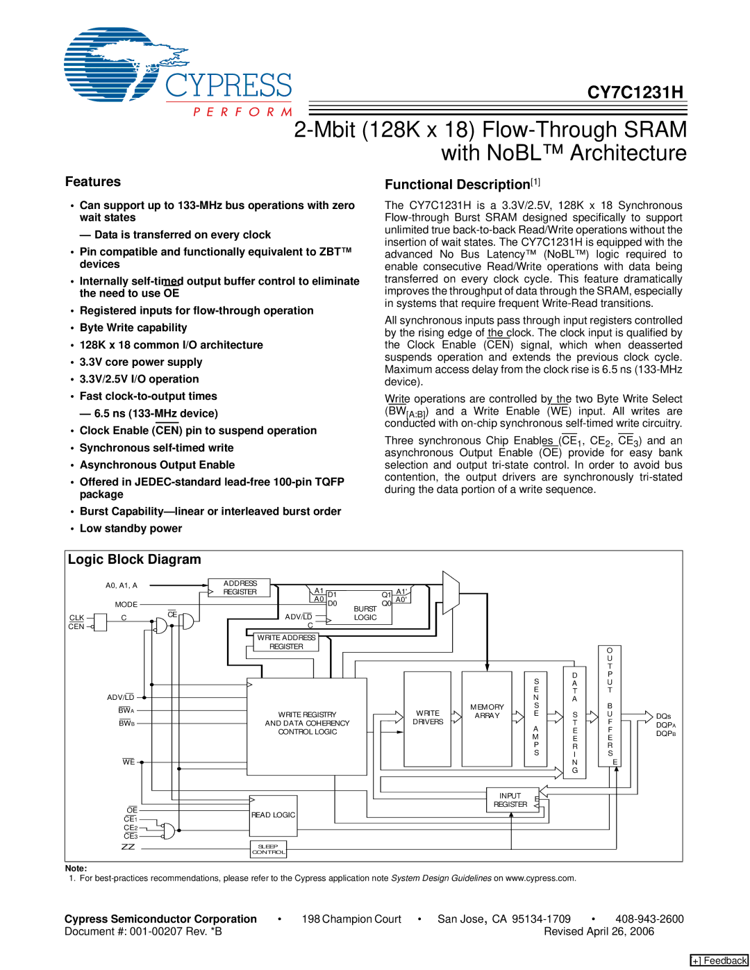
Logic Block Diagram |
|
|
|
|
|
|
|
|
|
| ||
| A0, A1, A |
| ADDRESS | A1 |
|
| A1' |
|
|
|
|
|
|
|
| REGISTER | D1 | Q1 |
|
|
|
|
| ||
| MODE |
|
| A0 | D0 | Q0 | A0' |
|
|
|
|
|
|
| CE |
| ADV/LD |
| BURST |
|
|
|
|
|
|
CLK | C |
|
| LOGIC |
|
|
|
|
|
| ||
|
|
|
|
|
|
|
|
| ||||
CEN |
|
|
| C |
|
|
|
|
|
|
|
|
|
|
|
| WRITE ADDRESS |
|
|
|
|
|
|
|
|
|
|
|
| REGISTER |
|
|
|
|
|
| O |
|
|
|
|
|
|
|
|
|
|
|
|
| |
|
|
|
|
|
|
|
|
|
|
| U |
|
|
|
|
|
|
|
|
|
|
|
| T |
|
|
|
|
|
|
|
|
|
| S | D | P |
|
|
|
|
|
|
|
|
|
| A | U |
| |
| ADV/LD |
|
|
|
|
|
|
| E | T | T |
|
|
|
|
|
|
|
|
| N | A |
|
| |
| BWA |
|
|
|
|
|
| MEMORY | S |
| B |
|
|
|
| WRITE REGISTRY |
| WRITE | ARRAY | E | S | U | DQs | ||
| BWB |
|
|
| ||||||||
|
|
| AND DATA COHERENCY |
| DRIVERS |
| A | T | F | DQPA | ||
|
|
|
| CONTROL LOGIC |
|
|
| E | F | DQPB | ||
|
|
|
|
|
|
| M | E | ||||
|
|
|
|
|
|
|
|
| E |
| ||
|
|
|
|
|
|
|
|
| P | R | R |
|
| WE |
|
|
|
|
|
|
| S | I | S | E |
|
|
|
|
|
|
|
|
| N |
| ||
|
|
|
|
|
|
|
|
|
| G |
|
|
|
|
|
|
|
|
|
| INPUT | E |
|
|
|
|
|
|
|
|
|
|
| REGISTER |
|
|
| |
| OE |
|
|
|
|
|
|
|
|
|
| |
|
| READ LOGIC |
|
|
|
|
|
|
|
| ||
| CE1 |
|
|
|
|
|
|
|
|
| ||
|
|
|
|
|
|
|
|
|
|
|
| |
| CE2 |
|
|
|
|
|
|
|
|
|
|
|
| CE3 |
|
|
|
|
|
|
|
|
|
|
|
| ZZ |
|
| SLEEP |
|
|
|
|
|
|
|
|
|
|
| CONTROL |
|
|
|
|
|
|
|
| |
Note: |
|
|
|
|
|
|
|
|
|
|
|
|
1. For
Cypress Semiconductor Corporation | • | 198 Champion Court • San Jose, CA | • | |
Document #: |
| Revised April 26, 2006 | ||
[+] Feedback