CY7C1334H
2-Mbit (64K x 32) Pipelined SRAM with NoBL™ Architecture
Features | Functional Description[1] |
•Pin compatible and functionally equivalent to ZBT™ devices
•Internally
•Byte Write capability
•64K x 32 common I/O architecture
•3.3V core power supply
•3.3V/2.5V I/O operation
•Fast
—3.5 ns (for
—4.0 ns (for
•Clock Enable (CEN) pin to suspend operation
•Synchronous
•Asynchronous output enable (OE)
•Offered in
•Burst
•“ZZ” Sleep mode option
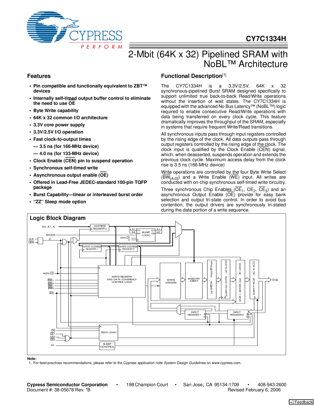
The CY7C1334H is a 3.3V/2.5V, 64K x 32
All synchronous inputs pass through input registers controlled by the rising edge of the clock. All data outputs pass through output registers controlled by the rising edge of the clock. The clock input is qualified by the Clock Enable (CEN) signal, which, when deasserted, suspends operation and extends the previous clock cycle. Maximum access delay from the clock rise is 3.5 ns
Write operations are controlled by the four Byte Write Select (BW[A:D]) and a Write Enable (WE) input. All writes are conducted with
Three synchronous Chip Enables (CE1, CE2, CE3) and an asynchronous Output Enable (OE) provide for easy bank selection and output
Logic Block Diagram |
|
|
|
|
|
|
|
|
|
| ||
| A0, A1, A | ADDRESS |
|
|
|
|
|
|
|
|
| |
|
| REGISTER 0 | A1 | D1 | Q1 A1' |
|
|
|
|
|
| |
|
|
|
|
|
|
|
|
|
| |||
| MODE |
|
| A0 | D0 BURST Q0 A0' |
|
|
|
|
|
| |
|
|
| ADV/LD |
| LOGIC |
|
|
|
|
|
| |
CLK | C |
|
|
|
|
|
|
|
|
|
| |
|
| C |
|
|
|
|
|
|
|
| ||
CEN |
|
|
|
|
|
|
|
|
|
|
| |
|
|
|
|
|
|
|
|
|
|
|
| |
|
| WRITE ADDRESS |
| WRITE ADDRESS |
|
|
|
|
|
|
| |
|
| REGISTER 1 |
| REGISTER 2 |
|
|
|
|
|
|
|
|
|
|
|
|
|
|
|
| S | O |
| O |
|
|
|
|
|
|
|
|
| U | D |
| ||
|
|
|
|
|
|
|
| E | T | U |
| |
|
|
|
|
|
|
|
| P | A | T |
| |
|
|
|
|
|
|
|
| N |
| |||
|
|
|
|
|
|
|
| U | T | P |
| |
| ADV/LD |
|
|
|
|
|
| S | T | A | U |
|
|
|
|
|
|
|
| R | T |
| |||
|
|
|
| WRITE REGISTRY |
|
| MEMORY | E | S | B |
| |
| BWA |
|
| AND DATA COHERENCY |
| WRITE |
| E | DQs | |||
|
|
|
| ARRAY |
| |||||||
| BWB |
|
| CONTROL LOGIC |
| DRIVERS | A | G | T | U |
| |
|
|
|
|
|
| I | F |
| ||||
| BWC |
|
|
|
|
|
| M | S | E |
| |
|
|
|
|
|
|
| F |
| ||||
| BWD |
|
|
|
|
|
| P | T | E | E |
|
|
|
|
|
|
|
|
| E | R |
| ||
| WE |
|
|
|
|
|
| S | R | R |
| |
|
|
|
|
|
|
|
|
| S | I | S |
|
|
|
|
|
|
|
|
|
| E | N | E |
|
|
|
|
|
|
|
|
|
|
| G |
|
|
|
|
|
|
|
|
| INPUT | E |
| INPUT | E |
|
|
|
|
|
|
|
| REGISTER 1 |
| REGISTER 0 |
| ||
| OE |
| READ LOGIC |
|
|
|
|
|
|
|
| |
| CE1 |
|
|
|
|
|
|
|
|
| ||
|
|
|
|
|
|
|
|
|
|
|
| |
| CE2 |
|
|
|
|
|
|
|
|
|
|
|
| CE3 |
|
|
|
|
|
|
|
|
|
|
|
| ZZ |
| SLEEP |
|
|
|
|
|
|
|
| |
| CONTROL |
|
|
|
|
|
|
|
| |||
|
|
|
|
|
|
|
|
|
| |||
Note: |
|
|
|
|
|
|
|
|
|
|
|
|
1. For
Cypress Semiconductor Corporation | • | 198 Champion Court • San Jose, CA | • | |
Document #: |
| Revised February 6, 2006 | ||
[+] Feedback