CY7C1334H
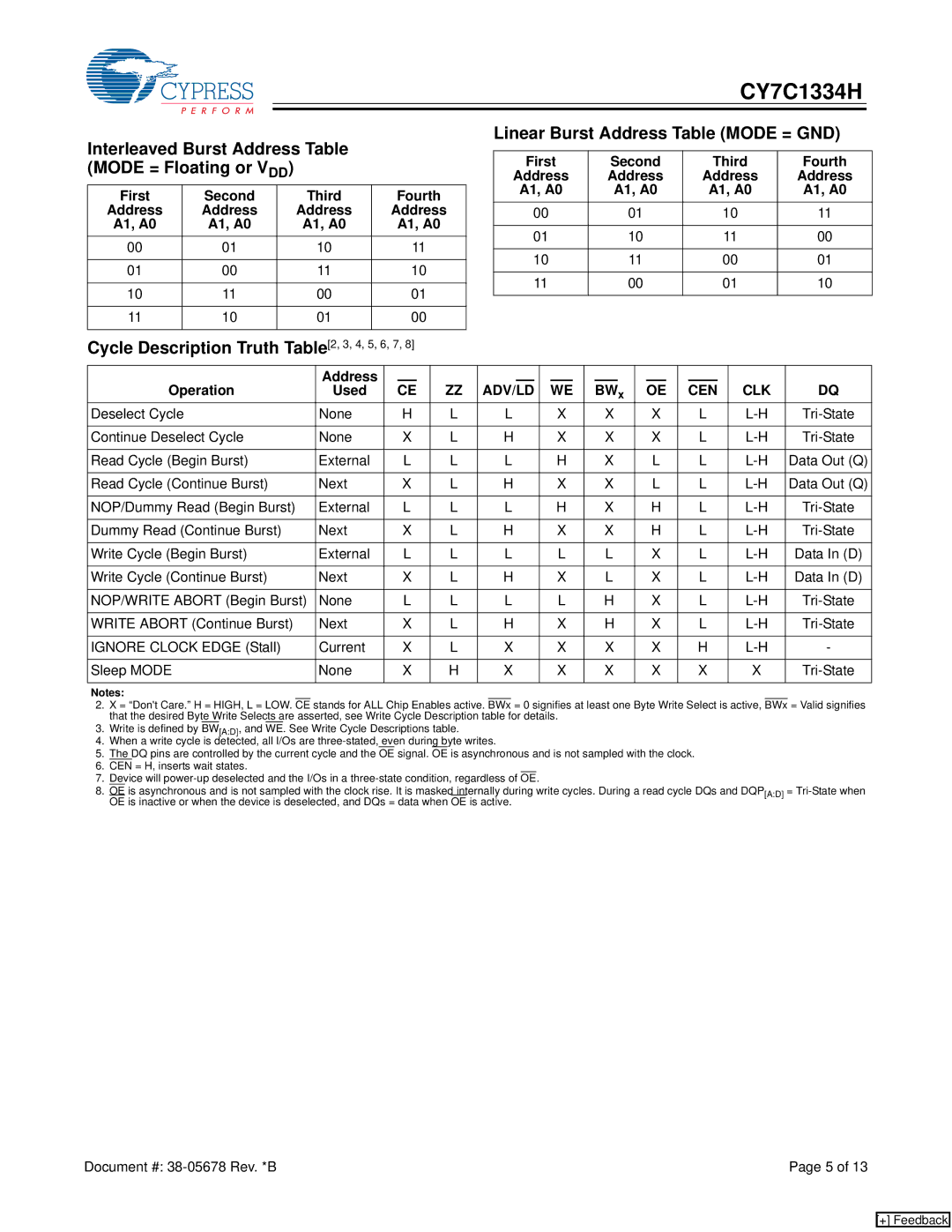
Interleaved Burst Address Table (MODE = Floating or VDD)
First | Second | Third | Fourth |
Address | Address | Address | Address |
A1, A0 | A1, A0 | A1, A0 | A1, A0 |
00 | 01 | 10 | 11 |
|
|
|
|
01 | 00 | 11 | 10 |
|
|
|
|
10 | 11 | 00 | 01 |
|
|
|
|
11 | 10 | 01 | 00 |
|
|
|
|
Cycle Description Truth Table[2, 3, 4, 5, 6, 7, 8]
Linear Burst Address Table (MODE = GND)
First | Second | Third | Fourth |
Address | Address | Address | Address |
A1, A0 | A1, A0 | A1, A0 | A1, A0 |
00 | 01 | 10 | 11 |
|
|
|
|
01 | 10 | 11 | 00 |
|
|
|
|
10 | 11 | 00 | 01 |
|
|
|
|
11 | 00 | 01 | 10 |
|
|
|
|
| Address |
|
|
|
|
|
|
|
|
|
|
|
|
|
|
|
|
|
|
|
|
|
Operation | Used |
| CE |
| ZZ | ADV/LD |
|
| WE |
|
| BWx |
| OE |
|
| CEN | CLK | DQ | |||
Deselect Cycle | None |
| H |
| L | L |
|
| X |
|
| X |
| X |
|
| L | |||||
|
|
|
|
|
|
|
|
|
|
|
|
|
|
|
|
|
|
|
| |||
Continue Deselect Cycle | None |
| X |
| L | H |
|
| X |
|
| X |
| X |
|
| L | |||||
|
|
|
|
|
|
|
|
|
|
|
|
|
|
|
|
|
|
|
| |||
Read Cycle (Begin Burst) | External |
| L |
| L | L |
|
| H |
|
| X |
| L |
|
| L | Data Out (Q) | ||||
|
|
|
|
|
|
|
|
|
|
|
|
|
|
|
|
|
|
|
| |||
Read Cycle (Continue Burst) | Next |
| X |
| L | H |
|
| X |
|
| X |
| L |
|
| L | Data Out (Q) | ||||
|
|
|
|
|
|
|
|
|
|
|
|
|
|
|
|
|
|
|
| |||
NOP/Dummy Read (Begin Burst) | External |
| L |
| L | L |
|
| H |
|
| X |
| H |
|
| L | |||||
|
|
|
|
|
|
|
|
|
|
|
|
|
|
|
|
|
|
|
| |||
Dummy Read (Continue Burst) | Next |
| X |
| L | H |
|
| X |
|
| X |
| H |
|
| L | |||||
|
|
|
|
|
|
|
|
|
|
|
|
|
|
|
|
|
|
|
| |||
Write Cycle (Begin Burst) | External |
| L |
| L | L |
|
| L |
|
| L |
| X |
|
| L | Data In (D) | ||||
|
|
|
|
|
|
|
|
|
|
|
|
|
|
|
|
|
|
|
| |||
Write Cycle (Continue Burst) | Next |
| X |
| L | H |
|
| X |
|
| L |
| X |
|
| L | Data In (D) | ||||
|
|
|
|
|
|
|
|
|
|
|
|
|
|
|
|
|
|
|
| |||
NOP/WRITE ABORT (Begin Burst) | None |
| L |
| L | L |
|
| L |
|
| H |
| X |
|
| L | |||||
|
|
|
|
|
|
|
|
|
|
|
|
|
|
|
|
|
|
|
| |||
WRITE ABORT (Continue Burst) | Next |
| X |
| L | H |
|
| X |
|
| H |
| X |
|
| L | |||||
|
|
|
|
|
|
|
|
|
|
|
|
|
|
|
|
|
|
|
| |||
IGNORE CLOCK EDGE (Stall) | Current |
| X |
| L | X |
|
| X |
|
| X |
| X |
|
| H | - | ||||
|
|
|
|
|
|
|
|
|
|
|
|
|
|
|
|
|
|
|
| |||
Sleep MODE | None |
| X |
| H | X |
|
| X |
|
| X |
| X |
|
| X | X | ||||
|
|
|
|
|
|
|
|
|
|
|
|
|
|
|
|
|
|
|
|
|
|
|
Notes:
2.X = “Don't Care.” H = HIGH, L = LOW. CE stands for ALL Chip Enables active. BWx = 0 signifies at least one Byte Write Select is active, BWx = Valid signifies that the desired Byte Write Selects are asserted, see Write Cycle Description table for details.
3.Write is defined by BW[A:D], and WE. See Write Cycle Descriptions table.
4.When a write cycle is detected, all I/Os are
5.The DQ pins are controlled by the current cycle and the OE signal. OE is asynchronous and is not sampled with the clock.
6.CEN = H, inserts wait states.
7.Device will
8.OE is asynchronous and is not sampled with the clock rise. It is masked internally during write cycles. During a read cycle DQs and DQP[A:D] =
Document #: | Page 5 of 13 |
[+] Feedback