CY7C1350G
On the subsequent clock rise the data lines are automatically
On the next clock rise the data presented to DQs and DQP[A:D] (or a subset for Byte Write operations, see Write Cycle Description table for details) inputs is latched into the device and the write is complete.
The data written during the Write operation is controlled by BW[A:D] signals. The CY7C1350G provides byte write capability that is described in the Write Cycle Description table. Asserting the Write Enable input (WE) with the selected Byte Write Select (BW[A:D]) input will selectively write to only the desired bytes. Bytes not selected during a Byte Write operation will remain unaltered. A synchronous
Because the CY7C1350G is a common I/O device, data should not be driven into the device while the outputs are active. The Output Enable (OE) can be deasserted HIGH before presenting data to the DQs and DQP[A:D] inputs. Doing so will
Burst Write Accesses
The CY7C1350G has an
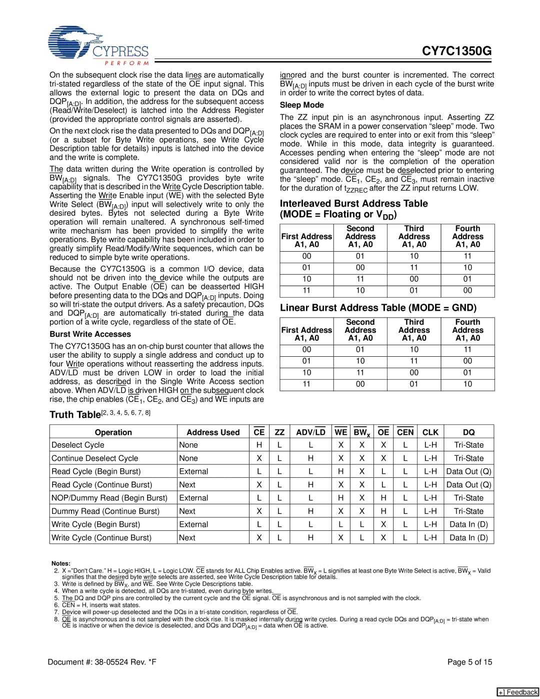
Truth Table[2, 3, 4, 5, 6, 7, 8]
ignored and the burst counter is incremented. The correct BW[A:D] inputs must be driven in each cycle of the burst write in order to write the correct bytes of data.
Sleep Mode
The ZZ input pin is an asynchronous input. Asserting ZZ places the SRAM in a power conservation “sleep” mode. Two clock cycles are required to enter into or exit from this “sleep” mode. While in this mode, data integrity is guaranteed. Accesses pending when entering the “sleep” mode are not considered valid nor is the completion of the operation guaranteed. The device must be deselected prior to entering the “sleep” mode. CE1, CE2, and CE3, must remain inactive for the duration of tZZREC after the ZZ input returns LOW.
Interleaved Burst Address Table (MODE = Floating or VDD)
First Address | Second | Third | Fourth |
Address | Address | Address | |
A1, A0 | A1, A0 | A1, A0 | A1, A0 |
00 | 01 | 10 | 11 |
01 | 00 | 11 | 10 |
10 | 11 | 00 | 01 |
11 | 10 | 01 | 00 |
Linear Burst Address Table (MODE = GND)
First Address | Second | Third | Fourth |
Address | Address | Address | |
A1, A0 | A1, A0 | A1, A0 | A1, A0 |
00 | 01 | 10 | 11 |
01 | 10 | 11 | 00 |
10 | 11 | 00 | 01 |
11 | 00 | 01 | 10 |
|
|
|
|
|
|
|
|
|
|
|
|
|
|
|
|
|
|
|
|
|
|
|
Operation | Address Used |
| CE |
| ZZ | ADV/LD |
|
| WE |
|
| BWx |
| OE |
|
| CEN | CLK | DQ | |||
Deselect Cycle | None |
| H |
| L | L |
|
| X |
|
| X |
| X |
|
| L | |||||
Continue Deselect Cycle | None |
| X |
| L | H |
|
| X |
|
| X |
| X |
|
| L | |||||
Read Cycle (Begin Burst) | External |
| L |
| L | L |
|
| H |
|
| X |
| L |
|
| L | Data Out (Q) | ||||
Read Cycle (Continue Burst) | Next |
| X |
| L | H |
|
| X |
|
| X |
| L |
|
| L | Data Out (Q) | ||||
NOP/Dummy Read (Begin Burst) | External |
| L |
| L | L |
|
| H |
|
| X |
| H |
|
| L | |||||
Dummy Read (Continue Burst) | Next |
| X |
| L | H |
|
| X |
|
| X |
| H |
|
| L | |||||
Write Cycle (Begin Burst) | External |
| L |
| L | L |
|
| L |
|
| L |
| X |
|
| L | Data In (D) | ||||
Write Cycle (Continue Burst) | Next |
| X |
| L | H |
|
| X |
|
| L |
| X |
|
| L | Data In (D) | ||||
Notes:
2.X =”Don't Care.” H = Logic HIGH, L = Logic LOW. CE stands for ALL Chip Enables active. BWx = L signifies at least one Byte Write Select is active, BWx = Valid signifies that the desired byte write selects are asserted, see Write Cycle Description table for details.
3.Write is defined by BWX, and WE. See Write Cycle Descriptions table.
4.When a write cycle is detected, all DQs are
5.The DQ and DQP pins are controlled by the current cycle and the OE signal. OE is asynchronous and is not sampled with the clock.
6.CEN = H, inserts wait states.
7.Device will
8.OE is asynchronous and is not sampled with the clock rise. It is masked internally during write cycles. During a read cycle DQs and DQP[A:D] =
Document #: | Page 5 of 15 |
[+] Feedback