CY7C1353G
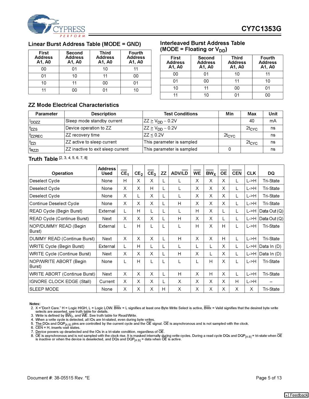
Linear Burst Address Table (MODE = GND)
First | Second | Third | Fourth |
Address | Address | Address | Address |
A1, A0 | A1, A0 | A1, A0 | A1, A0 |
00 | 01 | 10 | 11 |
|
|
|
|
01 | 10 | 11 | 00 |
|
|
|
|
10 | 11 | 00 | 01 |
|
|
|
|
11 | 00 | 01 | 10 |
|
|
|
|
Interleaved Burst Address Table (MODE = Floating or VDD)
First | Second | Third | Fourth |
Address | Address | Address | Address |
A1, A0 | A1, A0 | A1, A0 | A1, A0 |
00 | 01 | 10 | 11 |
|
|
|
|
01 | 00 | 11 | 10 |
|
|
|
|
10 | 11 | 00 | 01 |
|
|
|
|
11 | 10 | 01 | 00 |
|
|
|
|
ZZ Mode Electrical Characteristics
Parameter | Description |
|
|
|
|
|
|
| Test Conditions |
|
|
|
|
| Min |
| Max |
| Unit |
| |||||||||||
IDDZZ | Sleep mode standby current |
| ZZ > VDD − 0.2V |
|
|
|
|
|
|
|
|
|
|
|
|
|
| 40 |
| mA |
| ||||||||||
tZZS | Device operation to ZZ |
|
|
| ZZ > VDD − 0.2V |
|
|
|
|
|
|
|
|
|
|
|
|
|
| 2tCYC |
| ns |
| ||||||||
tZZREC | ZZ recovery time |
|
|
| ZZ < 0.2V |
|
|
|
|
|
|
|
|
|
| 2tCYC |
|
|
|
| ns |
| |||||||||
tZZI | ZZ active to sleep current |
|
|
| This parameter is sampled |
|
|
|
|
|
|
|
|
|
|
| 2tCYC |
| ns |
| |||||||||||
tRZZI | ZZ inactive to exit sleep current |
| This parameter is sampled |
|
|
|
|
|
| 0 |
|
|
|
|
| ns |
| ||||||||||||||
Truth Table [2, 3, 4, 5, 6, 7, 8] |
|
|
|
|
|
|
|
|
|
|
|
|
|
|
|
|
|
|
|
|
|
|
|
|
|
|
|
|
|
| |
|
| Address |
|
|
|
|
|
|
|
|
|
|
|
|
|
|
|
|
|
|
|
|
|
|
|
|
|
|
|
|
|
Operation | Used |
| CE | 1 | CE2 |
|
| CE | 3 | ZZ | ADV/LD |
|
| WE |
|
| BWX |
| OE |
|
| CEN | CLK |
| DQ | ||||||
Deselect Cycle |
| None |
| H | X |
|
| X | L | L |
|
| X |
|
| X |
| X |
|
| L | ||||||||||
Deselect Cycle |
| None |
| X | X |
|
| H | L | L |
|
| X |
|
| X |
| X |
|
| L | ||||||||||
Deselect Cycle |
| None |
| X | L |
|
| X | L | L |
|
| X |
|
| X |
| X |
|
| L | ||||||||||
Continue Deselect Cycle | None |
| X | X |
|
| X | L | H |
|
| X |
|
| X |
| X |
|
| L | |||||||||||
READ Cycle (Begin Burst) | External |
| L | H |
|
| L | L | L |
|
| H |
|
| X |
| L |
|
| L | Data Out (Q) | ||||||||||
READ Cycle (Continue Burst) | Next |
| X | X |
|
| X | L | H |
|
| X |
|
| X |
| L |
|
| L | Data Out (Q) | ||||||||||
NOP/DUMMY READ (Begin | External |
| L | H |
|
| L | L | L |
|
| H |
|
| X |
| H |
|
| L | |||||||||||
Burst) |
|
|
|
|
|
|
|
|
|
|
|
|
|
|
|
|
|
|
|
|
|
|
|
|
|
|
|
|
|
|
|
DUMMY READ (Continue Burst) | Next |
| X | X |
|
| X | L | H |
|
| X |
|
| X |
| H |
|
| L | |||||||||||
WRITE Cycle (Begin Burst) | External |
| L | H |
|
| L | L | L |
|
| L |
|
| L |
| X |
|
| L | Data In (D) | ||||||||||
WRITE Cycle (Continue Burst) | Next |
| X | X |
|
| X | L | H |
|
| X |
|
| L |
| X |
|
| L | Data In (D) | ||||||||||
NOP/WRITE ABORT (Begin | None |
| L | H |
|
| L | L | L |
|
| L |
|
| H |
| X |
|
| L | |||||||||||
Burst) |
|
|
|
|
|
|
|
|
|
|
|
|
|
|
|
|
|
|
|
|
|
|
|
|
|
|
|
|
|
|
|
WRITE ABORT (Continue Burst) | Next |
| X | X |
|
| X | L | H |
|
| X |
|
| H |
| X |
|
| L | |||||||||||
IGNORE CLOCK EDGE (Stall) | Current |
| X | X |
|
| X | L | X |
|
| X |
|
| X |
| X |
|
| H |
| – | |||||||||
SLEEP MODE |
| None |
| X | X |
|
| X | H | X |
|
| X |
|
| X |
| X |
|
| X | X | |||||||||
Notes:
2.X =”Don't Care.” H = Logic HIGH, L = Logic LOW. BWx = L signifies at least one Byte Write Select is active, BWx = Valid signifies that the desired byte write selects are asserted, see truth table for details.
3.Write is defined by BWX, and WE. See truth table for Read/Write.
4.When a write cycle is detected, all IOs are
5.The DQs and DQP[A:B] pins are controlled by the current cycle and the OE signal. OE is asynchronous and is not sampled with the clock.
6.CEN = H, inserts wait states.
7.Device powers up deselected and the IOs in a
8.OE is asynchronous and is not sampled with the clock rise. It is masked internally during write cycles. During a read cycle DQs and DQP[A:B] =
Document #: | Page 5 of 13 |
[+] Feedback