CY7C1354CV25


CY7C1356CV25


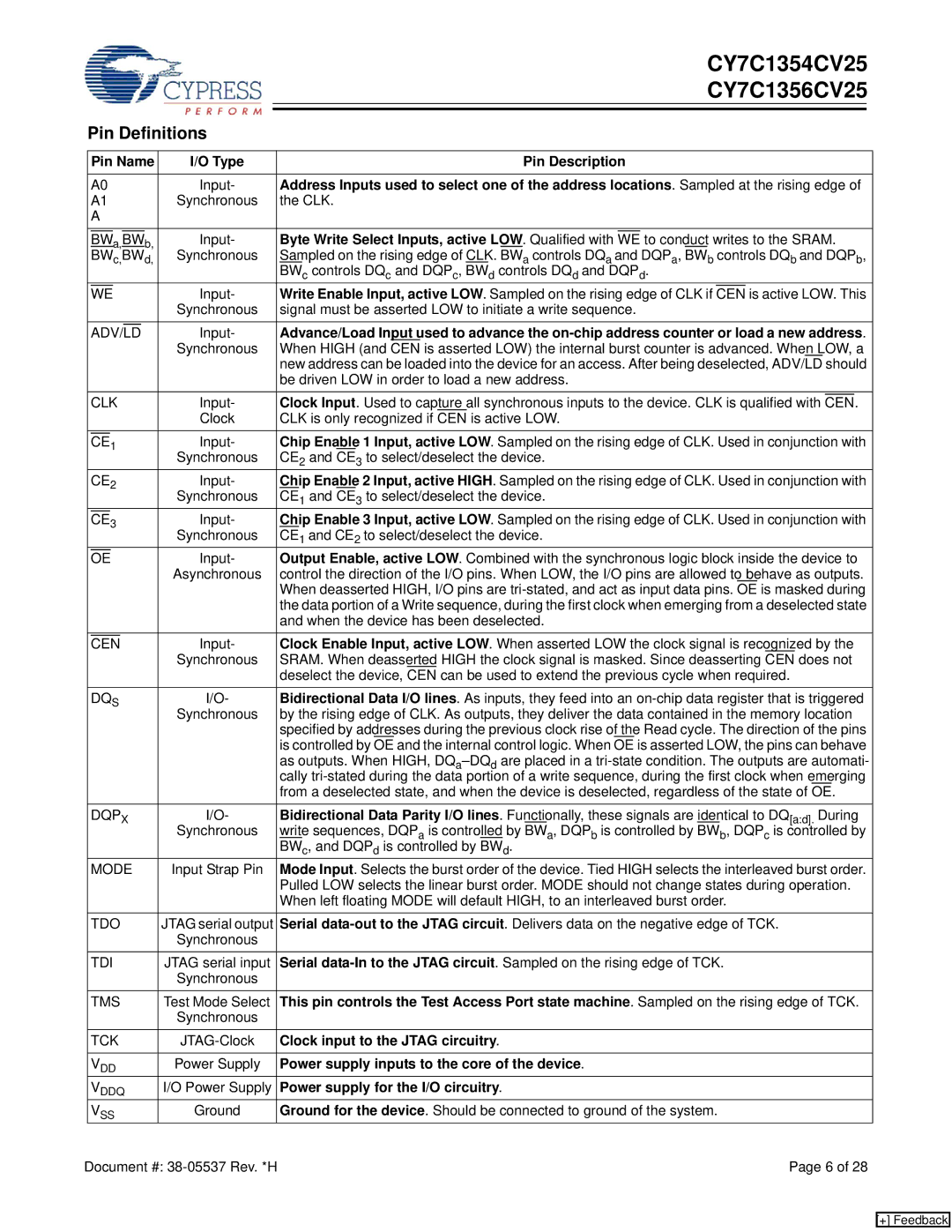
Pin Definitions


Pin Name

I/O Type


Pin Description


A0

Input-


Address Inputs used to select one of the address locations. Sampled at the rising edge of


A1

Synchronous


the CLK.


A


a,


b,

Input-


Byte Write Select Inputs, active LOW. Qualified with


to conduct writes to the SRAM.


BW

BW

WE


BWc,BWd,

Synchronous


Sampled on the rising edge of CLK. BWa controls DQa and DQPa, BWb controls DQb and DQPb,


BWc controls DQc and DQPc, BWd controls DQd and DQPd.


Input-


Write Enable Input, active LOW. Sampled on the rising edge of CLK if


is active LOW. This


WE

CEN


Synchronous


signal must be asserted LOW to initiate a write sequence.


Input-


Advance/Load Input used to advance the on-chip address counter or load a new address.


ADV/LD


Synchronous


When HIGH (and CEN is asserted LOW) the internal burst counter is advanced. When LOW, a


new address can be loaded into the device for an access. After being deselected, ADV/LD should


be driven LOW in order to load a new address.


CLK

Input-


Clock Input. Used to capture all synchronous inputs to the device. CLK is qualified with


CEN.


Clock


CLK is only recognized if CEN is active LOW.


1


Input-


Chip Enable 1 Input, active LOW. Sampled on the rising edge of CLK. Used in conjunction with


CE


Synchronous


CE2 and CE3 to select/deselect the device.


CE2

Input-


Chip Enable 2 Input, active HIGH. Sampled on the rising edge of CLK. Used in conjunction with


Synchronous


CE1 and CE3 to select/deselect the device.


3


Input-


Chip Enable 3 Input, active LOW. Sampled on the rising edge of CLK. Used in conjunction with


CE


Synchronous


CE1 and CE2 to select/deselect the device.


Input-


Output Enable, active LOW. Combined with the synchronous logic block inside the device to


OE


Asynchronous


control the direction of the I/O pins. When LOW, the I/O pins are allowed to behave as outputs.


When deasserted HIGH, I/O pins are tri-stated, and act as input data pins. OE is masked during


the data portion of a Write sequence, during the first clock when emerging from a deselected state


and when the device has been deselected.


Input-


Clock Enable Input, active LOW. When asserted LOW the clock signal is recognized by the


CEN


Synchronous


SRAM. When deasserted HIGH the clock signal is masked. Since deasserting CEN does not


deselect the device, CEN can be used to extend the previous cycle when required.


DQS

I/O-


Bidirectional Data I/O lines. As inputs, they feed into an on-chip data register that is triggered


Synchronous


by the rising edge of CLK. As outputs, they deliver the data contained in the memory location


specified by addresses during the previous clock rise of the Read cycle. The direction of the pins


is controlled by OE and the internal control logic. When OE is asserted LOW, the pins can behave


as outputs. When HIGH, DQa–DQdare placed in a tri-state condition. The outputs are automati-


cally tri-stated during the data portion of a write sequence, during the first clock when emerging


from a deselected state, and when the device is deselected, regardless of the state of OE.


DQPX

I/O-


Bidirectional Data Parity I/O lines. Functionally, these signals are identical to DQ[a:d]. During


Synchronous


write sequences, DQPa is controlled by BWa, DQPb is controlled by BWb, DQPc is controlled by


BWc, and DQPd is controlled by BWd.


MODE

Input Strap Pin


Mode Input. Selects the burst order of the device. Tied HIGH selects the interleaved burst order.


Pulled LOW selects the linear burst order. MODE should not change states during operation.


When left floating MODE will default HIGH, to an interleaved burst order.


TDO

JTAG serial output

Serial data-out to the JTAG circuit. Delivers data on the negative edge of TCK.


Synchronous


TDI

JTAG serial input


Serial data-In to the JTAG circuit. Sampled on the rising edge of TCK.


Synchronous


TMS

Test Mode Select


This pin controls the Test Access Port state machine. Sampled on the rising edge of TCK.


Synchronous


TCK

JTAG-Clock


Clock input to the JTAG circuitry.


VDD

Power Supply


Power supply inputs to the core of the device.


VDDQ

I/O Power Supply


Power supply for the I/O circuitry.


VSS

Ground


Ground for the device. Should be connected to ground of the system.

Document #: 38-05537 Rev. *H


Page 6 of 28

[+] Feedback

Page 6
Image 6
Cypress CY7C1356CV25, CY7C1354CV25 manual Pin Definitions

CY7C1356CV25, CY7C1354CV25 specifications

The Cypress CY7C1354CV25 and CY7C1356CV25 are high-performance, synchronous SRAM (Static Random Access Memory) devices designed for bandwidth-intensive applications. Both components are part of the Cypress family of low-power high-speed SRAMs, making them ideal for use in networking, telecommunications, and high-speed data processing systems.

One of the main features of the CY7C1354CV25 and CY7C1356CV25 is their wide data bus. The CY7C1354CV25 provides a 4 Megabit memory capacity with a 36-bit wide data interface, while the CY7C1356CV25 boosts this to 6 Megabits with a similarly wide data interface. This allows for high data throughput and efficiency in applications where quick access to large data sets is critical.

Both devices offer asynchronous write and synchronous read capabilities, enabling them to support pipelines and burst accesses effectively. The memory can be accessed in a single cycle, which considerably enhances performance in applications that require quick response times, such as high-speed packet processing in routers and switches.

The Cypress SRAMs are built using advanced CMOS technology, enabling low power consumption, which is essential for mobile and battery-operated devices. Their operating voltage range, typically between 2.7V and 3.6V, contributes to the low power profile while providing a high level of performance.

Moreover, both devices support a wide temperature range, making them suitable for industrial applications. They can operate in environments from -40°C to +125°C, ensuring reliability and performance under varying conditions. This makes the CY7C1354CV25 and CY7C1356CV25 particularly valuable for automotive and aerospace applications where temperature extremes can be encountered.

Cypress has enhanced the reliability of these SRAMs with features such as built-in error detection and correction capabilities. This ensures data integrity, which is crucial for mission-critical applications.

In summary, the Cypress CY7C1354CV25 and CY7C1356CV25 ensure tight integration of high capacity, speed, and reliability. With their advanced synchronous architecture, low power consumption, and broad temperature range, they represent an excellent choice for applications that demand high performance in challenging environments. These SRAM devices continue to meet the needs of modern electronic designs, making them a trusted solution in the industry.