CY7C1416AV18, CY7C1427AV18
CY7C1418AV18, CY7C1420AV18
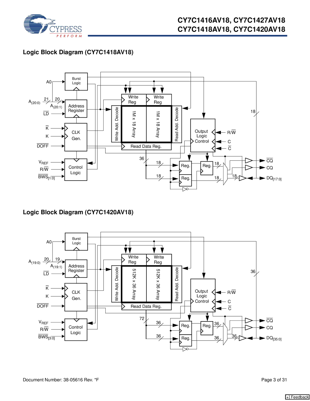
Logic Block Diagram (CY7C1418AV18)
|
|
| A0 |
|
|
| Burst |
|
|
| |||
|
|
|
|
| Logic |
|
|
| |||||
|
|
|
|
|
|
|
| ||||||
|
|
|
|
|
|
|
| ||||||
| 21 |
| 20 |
|
|
|
|
|
|
| |||
|
|
|
|
|
|
|
| ||||||
A(20:0) |
|
|
| A(20:1) | Address |
|
|
| |||||
|
|
|
|
|
|
|
|
| Register |
|
|
| |
|
|
|
|
|
|
|
|
|
|
|
| ||
|
| LD |
|
|
|
|
|
|
|
| |||
|
|
|
|
|
|
|
|
|
|
|
| ||
|
|
|
|
|
|
|
|
|
|
|
|
|
|
|
|
|
|
|
|
|
|
|
|
|
|
|
|
K
CLK
K![]()
![]()
![]()
![]() Gen.
Gen.
DOFF 

VREF |
|
|
|
|
|
| ||
|
| Control |
| |||||
|
| |||||||
|
|
|
|
|
|
| ||
R/W |
|
|
| |||||
|
| Logic |
| |||||
|
|
|
|
|
|
| ||
BWS |
|
|
|
|
|
| ||
[1:0] |
|
|
| |||||
| Write | Write |
|
|
|
Decode | Reg | Reg | Decode |
|
|
1M x | 1M x |
| 18 | ||
WriteAdd. | 18Array | 18Array | ReadAdd. | Logic |
|
|
|
|
| Output | R/W |
| Read Data Reg. |
| Control | C | |
|
|
| C | ||
|
|
|
|
| |
36 |
|
|
|
|
|
|
|
|
|
|
|
|
|
|
|
|
|
|
|
|
|
|
|
|
|
|
|
|
|
|
|
|
|
|
|
|
|
|
|
|
|
|
|
|
|
|
|
|
|
|
|
|
|
|
|
| |
| 18 |
|
|
| Reg. |
|
| Reg. | 18 |
|
|
|
|
|
|
|
|
|
|
| CQ | |||||||
|
|
|
|
|
|
|
|
|
|
|
|
|
|
|
| CQ | ||||||||||||
18 |
|
|
|
|
|
|
|
|
|
|
|
|
|
|
|
|
|
| 18 |
|
|
|
|
|
| |||
|
|
|
|
|
|
|
|
|
|
|
|
|
|
|
|
|
|
|
|
|
|
|
|
|
| |||
|
|
|
|
|
|
|
|
|
|
|
|
|
|
|
|
|
|
|
|
|
|
|
|
| ||||
|
|
|
|
| Reg. |
| 18 |
|
|
|
|
|
|
|
|
|
|
| DQ[17:0] | |||||||||
|
|
|
|
|
|
|
|
|
|
|
| |||||||||||||||||
|
|
|
|
|
|
|
|
| ||||||||||||||||||||
|
|
|
|
|
|
|
|
|
|
|
|
|
|
|
|
|
|
|
|
|
|
|
|
|
|
|
|
|
|
|
|
|
|
|
|
|
|
|
|
|
|
|
|
|
|
|
|
|
|
|
|
|
|
|
|
|
|
|
|
|
|
|
|
|
|
|
|
|
|
|
|
|
|
|
|
|
|
|
|
|
|
|
|
|
|
|
Logic Block Diagram (CY7C1420AV18)
|
|
| A0 |
|
|
| Burst |
|
|
| |||
|
|
|
|
| Logic |
|
|
| |||||
|
|
|
|
|
|
|
| ||||||
|
|
|
|
|
|
|
| ||||||
| 20 |
| 19 |
|
|
|
|
|
|
| |||
|
|
|
|
|
|
|
| ||||||
A(19:0) |
|
|
| A(19:1) | Address |
|
|
| |||||
|
|
|
|
|
|
|
|
| Register |
|
|
| |
|
|
|
|
|
|
|
|
|
|
|
| ||
|
| LD |
|
|
|
|
|
|
|
| |||
|
|
|
|
|
|
|
|
|
|
|
| ||
|
|
|
|
|
|
|
|
|
|
|
|
|
|
|
|
|
|
|
|
|
|
|
|
|
|
|
|
K
CLK
K![]()
![]()
![]()
![]() Gen.
Gen.
DOFF 

VREF |
|
|
|
|
|
| ||
|
| Control |
| |||||
|
| |||||||
|
|
|
|
|
|
| ||
R/W |
|
|
| |||||
|
| Logic |
| |||||
|
|
|
|
|
|
| ||
BWS |
|
|
|
|
|
| ||
[3:0] |
|
|
| |||||
| Write | Write |
|
|
|
DecodeAdd.Write | Reg | Reg | DecodeAdd.Read |
|
|
512Kx36Array | 512Kx36Array | Logic | 36 | ||
|
|
|
|
| |
|
|
|
| Output | R/W |
| Read Data Reg. |
| Control | C | |
|
|
| C | ||
|
|
|
|
| |
72 |
|
|
|
|
|
|
|
|
|
|
|
|
|
|
|
|
|
|
|
|
|
|
|
|
|
|
|
|
|
|
|
|
|
|
|
|
|
|
|
|
|
|
|
|
|
|
|
|
|
|
|
|
|
|
|
| |
| 36 |
|
|
| Reg. |
|
| Reg. | 36 |
|
|
|
|
|
|
|
|
|
|
| CQ | |||||||
|
|
|
|
|
|
|
|
|
|
|
|
|
|
|
| CQ | ||||||||||||
36 |
|
|
|
|
|
|
|
|
|
|
|
|
|
|
|
|
|
| 36 |
|
|
|
|
|
| |||
|
|
|
|
|
|
|
|
|
|
|
|
|
|
|
|
|
|
|
|
|
|
|
|
|
| |||
|
|
|
|
|
|
|
|
|
|
|
|
|
|
|
|
|
|
|
|
|
|
|
|
| ||||
|
|
|
|
| Reg. |
| 36 |
|
|
|
|
|
|
|
|
|
|
| DQ[35:0] | |||||||||
|
|
|
|
|
|
|
|
|
|
|
| |||||||||||||||||
|
|
|
|
|
|
|
|
| ||||||||||||||||||||
|
|
|
|
|
|
|
|
|
|
|
|
|
|
|
|
|
|
|
|
|
|
|
|
|
|
|
|
|
|
|
|
|
|
|
|
|
|
|
|
|
|
|
|
|
|
|
|
|
|
|
|
|
|
|
|
|
|
|
|
|
|
|
|
|
|
|
|
|
|
|
|
|
|
|
|
|
|
|
|
|
|
|
|
|
|
|
Document Number: | Page 3 of 31 |
[+] Feedback