CY7C1510JV18, CY7C1525JV18
CY7C1512JV18, CY7C1514JV18
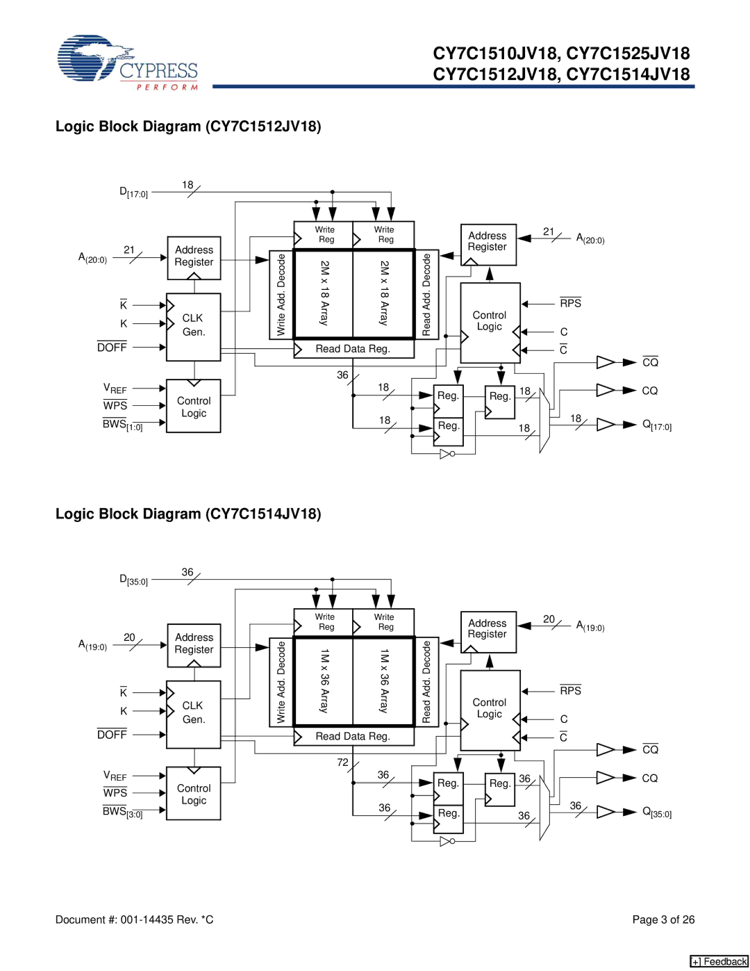
Logic Block Diagram (CY7C1512JV18)
18
D[17:0]
Write | Write |
Reg | Reg |
21 | Address | Add.WriteDecode | 2M x 18Array | 2M x 18Array |
A(20:0) | Gen. | |||
Register |
|
|
| |
K | CLK |
|
|
|
K |
|
|
| |
|
|
|
|
DOFF |
|
|
|
|
|
|
|
|
| Read Data Reg. | |||
|
|
|
|
|
|
| |||||||
|
|
|
|
| |||||||||
|
|
|
|
|
|
|
|
|
|
|
|
|
|
|
|
|
|
|
|
|
|
|
|
|
|
| |
| VREF |
|
|
|
|
|
| 36 | 18 | ||||
|
|
| Control |
|
|
|
| ||||||
|
|
|
|
|
| ||||||||
|
|
|
|
|
|
|
|
|
|
|
| ||
| WPS |
|
|
|
|
|
|
|
|
| |||
|
|
| Logic |
|
|
|
| 18 | |||||
|
|
|
|
|
|
|
|
|
|
| |||
|
|
|
|
|
|
|
|
|
|
|
|
| |
| BWS[1:0] |
|
|
|
|
|
| ||||||
|
|
|
|
|
|
|
| ||||||
![]() Read Add. Decode
Read Add. Decode
![]() Reg.
Reg.
![]() Reg.
Reg.
Address Register
Control
Logic
Reg.
21 A(20:0)
RPS
C
C
CQ
18 ![]()
![]()
![]()
![]() CQ
CQ
18 | 18 | Q[17:0] |
|
Logic Block Diagram (CY7C1514JV18)
36
D[35:0]
Write | Write |
Reg | Reg |
20 | Address | Add.WriteDecode | 1M x 36Array | 1M x 36Array |
A(19:0) | Gen. | |||
Register |
|
|
| |
K | CLK |
|
|
|
K |
|
|
| |
|
|
|
|
DOFF |
|
|
|
|
|
|
|
|
| Read Data Reg. | |||
|
|
|
|
|
|
| |||||||
|
|
|
|
| |||||||||
|
|
|
|
|
|
|
|
|
|
|
|
|
|
|
|
|
|
|
|
|
|
|
|
|
|
| |
| VREF |
|
|
|
|
|
| 72 | 36 | ||||
|
|
| Control |
|
|
|
| ||||||
|
|
|
|
|
| ||||||||
|
|
|
|
|
|
|
|
|
|
|
| ||
| WPS |
|
|
|
|
|
|
|
|
| |||
|
|
| Logic |
|
|
|
| 36 | |||||
|
|
|
|
|
|
|
|
|
|
| |||
|
|
|
|
|
|
|
|
|
|
|
|
| |
| BWS[3:0] |
|
|
|
|
|
| ||||||
|
|
|
|
|
|
|
| ||||||
![]() Read Add. Decode
Read Add. Decode
![]() Reg.
Reg.
![]() Reg.
Reg.
Address Register
Control
Logic
Reg.
20 A(19:0)
RPS
C
C
CQ
36 ![]()
![]()
![]()
![]() CQ
CQ
36 | 36 | Q[35:0] |
|
Document #: | Page 3 of 26 |
[+] Feedback