CY7C1510JV18, CY7C1525JV18
CY7C1512JV18, CY7C1514JV18
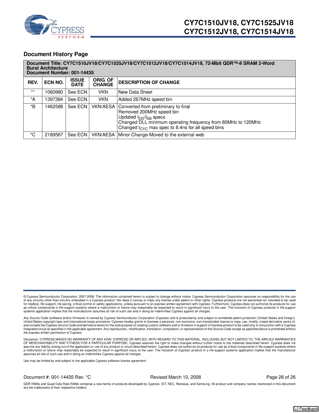
Document History Page
Document Title: CY7C1510JV18/CY7C1525JV18/CY7C1512JV18/CY7C1514JV18,
Burst Architecture
Document Number:
REV. | ECN NO. | ISSUE | ORIG. OF | DESCRIPTION OF CHANGE |
DATE | CHANGE | |||
|
|
|
|
|
** | 1060980 | See ECN | VKN | New Data Sheet |
|
|
|
|
|
*A | 1397384 | See ECN | VKN | Added 267MHz speed bin |
|
|
|
|
|
*B | 1462588 | See ECN | VKN/AESA | Converted from preliminary to final |
|
|
|
| Removed 200MHz speed bin |
|
|
|
| Updated IDD/ISB specs |
|
|
|
| Changed DLL minimum operating frequency from 80MHz to 120MHz |
|
|
|
| Changed tCYC max spec to 8.4ns for all speed bins |
*C | 2189567 | See ECN | VKN/AESA | Minor |
|
|
|
|
|
© Cypress Semiconductor Corporation,
Any Source Code (software and/or firmware) is owned by Cypress Semiconductor Corporation (Cypress) and is protected by and subject to worldwide patent protection (United States and foreign), United States copyright laws and international treaty provisions. Cypress hereby grants to licensee a personal,
Disclaimer: CYPRESS MAKES NO WARRANTY OF ANY KIND, EXPRESS OR IMPLIED, WITH REGARD TO THIS MATERIAL, INCLUDING, BUT NOT LIMITED TO, THE IMPLIED WARRANTIES OF MERCHANTABILITY AND FITNESS FOR A PARTICULAR PURPOSE. Cypress reserves the right to make changes without further notice to the materials described herein. Cypress does not assume any liability arising out of the application or use of any product or circuit described herein. Cypress does not authorize its products for use as critical components in
Use may be limited by and subject to the applicable Cypress software license agreement.
Document #: | Revised March 10, 2008 | Page 26 of 26 |
QDR RAMs and Quad Data Rate RAMs comprise a new family of products developed by Cypress, IDT, NEC, Renesas, and Samsung. All product and company names mentioned in this document are the trademarks of their respective holders.
[+] Feedback