CY7C1510JV18, CY7C1525JV18 CY7C1512JV18, CY7C1514JV18
Maximum Ratings
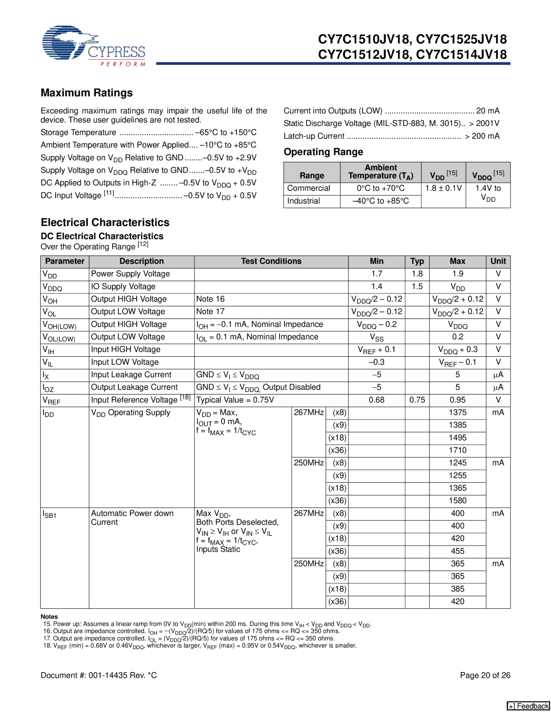
Exceeding maximum ratings may impair the useful life of the device. These user guidelines are not tested.
Storage Temperature | ||
Ambient Temperature with Power Applied | .... | |
Supply Voltage on VDD Relative to GND | ||
Supply Voltage on VDDQ Relative to GND | ||
DC Applied to Outputs in | ||
DC Input Voltage [11] | ||
|
| DD |
Current into Outputs (LOW) |
| 20 mA | ||
Static Discharge Voltage | > 2001V | |||
................................................... |
| > 200 mA | ||
Operating Range |
|
| ||
|
|
|
|
|
|
| Ambient | VDD [15] | VDDQ [15] |
Range |
| Temperature (TA) | ||
Commercial |
| 0°C to +70°C | 1.8 ± 0.1V | 1.4V to |
|
|
|
| VDD |
Industrial |
|
| ||
Electrical Characteristics
DC Electrical Characteristics
Over the Operating Range [12]
Parameter | Description | Test Conditions |
| Min | Typ | Max | Unit | |
VDD | Power Supply Voltage |
|
|
| 1.7 | 1.8 | 1.9 | V |
VDDQ | IO Supply Voltage |
|
|
| 1.4 | 1.5 | VDD | V |
VOH | Output HIGH Voltage | Note 16 |
|
| VDDQ/2 – 0.12 |
| VDDQ/2 + 0.12 | V |
VOL | Output LOW Voltage | Note 17 |
|
| VDDQ/2 – 0.12 |
| VDDQ/2 + 0.12 | V |
VOH(LOW) | Output HIGH Voltage | IOH = −0.1 mA, Nominal Impedance |
| VDDQ – 0.2 |
| VDDQ | V | |
VOL(LOW) | Output LOW Voltage | IOL = 0.1 mA, Nominal Impedance |
| VSS |
| 0.2 | V | |
VIH | Input HIGH Voltage |
|
|
| VREF + 0.1 |
| VDDQ + 0.3 | V |
VIL | Input LOW Voltage |
|
|
|
| VREF – 0.1 | V | |
IX | Input Leakage Current | GND ≤ VI ≤ VDDQ |
|
| −5 |
| 5 | μA |
IOZ | Output Leakage Current | GND ≤ VI ≤ VDDQ, Output Disabled |
| −5 |
| 5 | μA | |
VREF | Input Reference Voltage [18] | Typical Value = 0.75V |
|
| 0.68 | 0.75 | 0.95 | V |
IDD | VDD Operating Supply | VDD = Max, | 267MHz | (x8) |
|
| 1375 | mA |
|
| IOUT = 0 mA, |
|
|
|
|
|
|
|
|
| (x9) |
|
| 1385 |
| |
|
| f = fMAX = 1/tCYC |
|
|
|
|
|
|
|
|
| (x18) |
|
| 1495 |
| |
|
|
|
|
|
|
| ||
|
|
|
|
|
|
|
|
|
|
|
|
| (x36) |
|
| 1710 |
|
|
|
|
|
|
|
|
|
|
|
|
| 250MHz | (x8) |
|
| 1245 | mA |
|
|
|
|
|
|
|
|
|
|
|
|
| (x9) |
|
| 1255 |
|
|
|
|
|
|
|
|
|
|
|
|
|
| (x18) |
|
| 1365 |
|
|
|
|
|
|
|
|
|
|
|
|
|
| (x36) |
|
| 1580 |
|
|
|
|
|
|
|
|
|
|
ISB1 | Automatic Power down | Max VDD, | 267MHz | (x8) |
|
| 400 | mA |
| Current | Both Ports Deselected, |
|
|
|
|
|
|
|
| (x9) |
|
| 400 |
| ||
|
| VIN ≥ VIH or VIN ≤ VIL |
|
|
|
| ||
|
|
|
|
|
|
|
| |
|
|
| (x18) |
|
| 420 |
| |
|
| f = fMAX = 1/tCYC, |
|
|
|
| ||
|
| Inputs Static |
| (x36) |
|
| 455 |
|
|
|
|
|
|
|
|
|
|
|
|
| 250MHz | (x8) |
|
| 365 | mA |
|
|
|
|
|
|
|
|
|
|
|
|
| (x9) |
|
| 365 |
|
|
|
|
|
|
|
|
|
|
|
|
|
| (x18) |
|
| 385 |
|
|
|
|
|
|
|
|
|
|
|
|
|
| (x36) |
|
| 420 |
|
|
|
|
|
|
|
|
|
|
Notes
15.Power up: Assumes a linear ramp from 0V to VDD(min) within 200 ms. During this time VIH < VDD and VDDQ < VDD.
16.Output are impedance controlled. IOH = −(VDDQ/2)/(RQ/5) for values of 175 ohms <= RQ <= 350 ohms.
17.Output are impedance controlled. IOL = (VDDQ/2)/(RQ/5) for values of 175 ohms <= RQ <= 350 ohms.
18.VREF (min) = 0.68V or 0.46VDDQ, whichever is larger, VREF (max) = 0.95V or 0.54VDDQ, whichever is smaller.
Document #: | Page 20 of 26 |
[+] Feedback
