CY7C68003
Functional Overview
UTMI+ Low Pin Interface (ULPI)
This block conforms to the ULPI Specification. It supports the
Oscillator (OSC)
This block meets the requirements of both the
■Integrated Crystal Oscillator - 13, 19.2, 24, or 26 MHz crystal
■13, 19.2, 24, or 26 MHz LVCMOS single ended input clock on XI
Phase Locked Loop (PLL)
The PLL meets all clock stability requirements imposed by this device and the USB standard. It supports all requirements to make the device compliant to the USB 2.0 specifications. It also has a fractional multiplier that enables it to supply the correct frequency to the device when it is presented with a 13, 19.2, 24, or 26 MHz reference clock.
Power On Reset (POR)
This block provides a power on reset signal (internal) based on the input supply. An internal power on reset is generated when VCC input rises above VPOR(trip).
Reset (RESET_N)
The three major functions of RESET_N pin are as follows:
■Reset TX2UL
■Place TX2UL into Sleep Mode
■Place TX2UL into Configuration Mode
When the RESET_N pin is asserted (low) for tSTATE (tSTATE is specified in Table 21 on page 19), the TX2UL enters into either Sleep Mode or Configuration Mode depending on the CS_N state. When RESET_N is asserted while CS_N is asserted, TX2UL enters into Sleep Mode. When RESET_N is asserted for tSTATE while CS_N is deasserted, TX2UL enters into Configu- ration Mode. In these modes, all the pins in the ULPI interface are
■
■Associate with RESET_N to place TX2UL in the Sleep mode
When the CS_N pin is deasserted (high), all the pins in the ULPI interface are
USB2 Transceiver Macrocell Interface (UTMI+)
This block conforms to the UTMI+ Level 0 standard. It performs all the UTMI to USB translation.
Global Control
This block is the digital control logic that ties the blocks of the device together. Functions performed include pull up control, over current protect control, and more.
Full Speed and High Speed USB Transceivers (FS/HS)
The FS and HS Transceivers comply fully with the USB 2.0 specifications.
USB Pull up and Intr Detect, Termination Resistors (Pull up / TERM)
These blocks contain the USB pull up and termination resistors as specified by the USB 2.0 specification.
UART Pass Through Mode
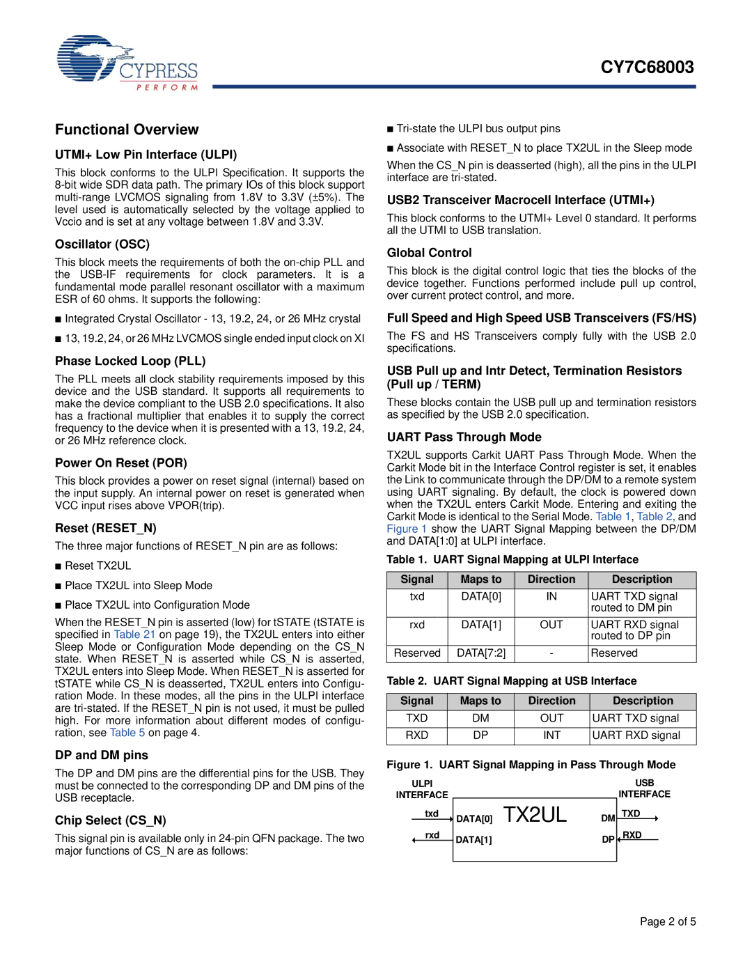
TX2UL supports Carkit UART Pass Through Mode. When the Carkit Mode bit in the Interface Control register is set, it enables the Link to communicate through the DP/DM to a remote system using UART signaling. By default, the clock is powered down when the TX2UL enters Carkit Mode. Entering and exiting the Carkit Mode is identical to the Serial Mode. Table 1, Table 2, and Figure 1 show the UART Signal Mapping between the DP/DM and DATA[1:0] at ULPI interface.
Table 1. UART Signal Mapping at ULPI Interface
Signal | Maps to | Direction | Description |
txd | DATA[0] | IN | UART TXD signal |
|
|
| routed to DM pin |
rxd | DATA[1] | OUT | UART RXD signal |
|
|
| routed to DP pin |
Reserved | DATA[7:2] | - | Reserved |
|
|
|
|
Table 2. UART Signal Mapping at USB Interface | |||
|
|
|
|
Signal | Maps to | Direction | Description |
TXD | DM | OUT | UART TXD signal |
|
|
|
|
RXD | DP | INT | UART RXD signal |
|
|
|
|
DP and DM pins
The DP and DM pins are the differential pins for the USB. They must be connected to the corresponding DP and DM pins of the USB receptacle.
Chip Select (CS_N)
This signal pin is available only in
Figure 1. UART Signal Mapping in Pass Through Mode
ULPI |
|
|
| USB | |||||
INTERFACE |
|
| INTERFACE | ||||||
|
| txd |
| DATA[0] TX2UL | DM |
| TXD |
|
|
|
| rxd |
| RXD | |||||
|
| DATA[1] | DP |
|
| ||||
|
|
|
| ||||||
|
|
|
|
|
|
|
|
|
|
Page 2 of 5