CY7C68003
Clocking
TX2UL supports external crystal and clock inputs at the 13, 19.2, 24, and 26 MHz frequencies. The internal PLL applies the proper clock multiply option depending on the input frequency. For appli- cations that use an external clock source to drive XI, the XO pin (in
■Parallel Resonant
■Fundamental Mode
■750 mW Drive Level
■12 pF (5 percent tolerance) Load Capacitors
■150 ppm
TX2UL operates on one of two primary clock sources:
■LVCMOS square wave clock input driven on the XI pin
■Crystal generated sine wave clock on the XI and XO pins
Table 3. External Clock Requirements
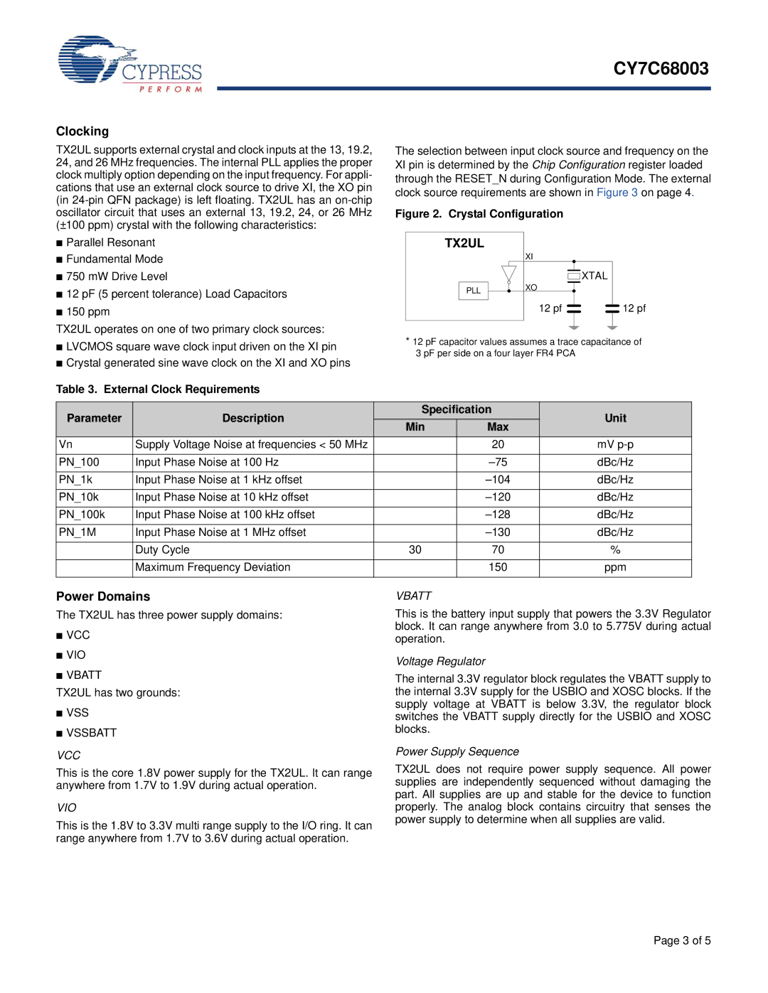
The selection between input clock source and frequency on the XI pin is determined by the Chip Configuration register loaded through the RESET_N during Configuration Mode. The external clock source requirements are shown in Figure 3 on page 4.
Figure 2. Crystal Configuration
TX2UL
XI

 XTAL
XTAL
PLL | XO |
|
12 pf |
|
|
|
|
| 12 pf |
|
|
|
| |||
|
|
|
|
|
|
|
*12 pF capacitor values assumes a trace capacitance of 3 pF per side on a four layer FR4 PCA
Parameter | Description | Specification | Unit | ||
Min | Max | ||||
|
|
| |||
Vn | Supply Voltage Noise at frequencies < 50 MHz |
| 20 | mV | |
|
|
|
|
| |
PN_100 | Input Phase Noise at 100 Hz |
| dBc/Hz | ||
|
|
|
|
| |
PN_1k | Input Phase Noise at 1 kHz offset |
| dBc/Hz | ||
|
|
|
|
| |
PN_10k | Input Phase Noise at 10 kHz offset |
| dBc/Hz | ||
|
|
|
|
| |
PN_100k | Input Phase Noise at 100 kHz offset |
| dBc/Hz | ||
|
|
|
|
| |
PN_1M | Input Phase Noise at 1 MHz offset |
| dBc/Hz | ||
|
|
|
|
| |
| Duty Cycle | 30 | 70 | % | |
|
|
|
|
| |
| Maximum Frequency Deviation |
| 150 | ppm | |
|
|
|
|
| |
Power Domains
The TX2UL has three power supply domains:
■VCC
■VIO
■VBATT
TX2UL has two grounds:
■VSS
■VSSBATT
VCC
This is the core 1.8V power supply for the TX2UL. It can range anywhere from 1.7V to 1.9V during actual operation.
VIO
This is the 1.8V to 3.3V multi range supply to the I/O ring. It can range anywhere from 1.7V to 3.6V during actual operation.
VBATT
This is the battery input supply that powers the 3.3V Regulator block. It can range anywhere from 3.0 to 5.775V during actual operation.
Voltage Regulator
The internal 3.3V regulator block regulates the VBATT supply to the internal 3.3V supply for the USBIO and XOSC blocks. If the supply voltage at VBATT is below 3.3V, the regulator block switches the VBATT supply directly for the USBIO and XOSC blocks.
Power Supply Sequence
TX2UL does not require power supply sequence. All power supplies are independently sequenced without damaging the part. All supplies are up and stable for the device to function properly. The analog block contains circuitry that senses the power supply to determine when all supplies are valid.
Page 3 of 5