PRELIMINARYCY7C656xx
7.0Pin Description Table
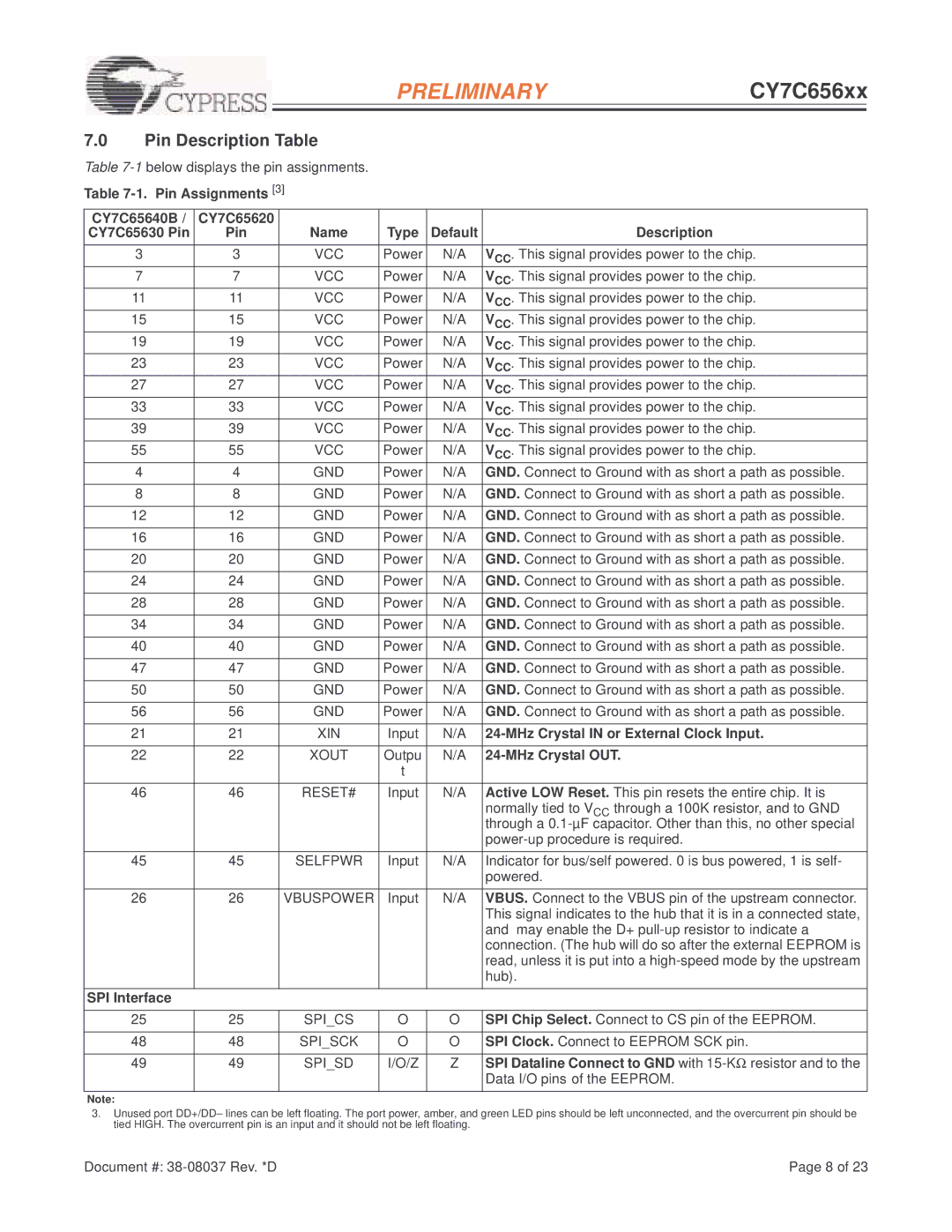
Table
Table
CY7C65640B / | CY7C65620 |
|
|
|
|
CY7C65630 Pin | Pin | Name | Type | Default | Description |
|
|
|
|
|
|
3 | 3 | VCC | Power | N/A | VCC. This signal provides power to the chip. |
7 | 7 | VCC | Power | N/A | VCC. This signal provides power to the chip. |
11 | 11 | VCC | Power | N/A | VCC. This signal provides power to the chip. |
15 | 15 | VCC | Power | N/A | VCC. This signal provides power to the chip. |
19 | 19 | VCC | Power | N/A | VCC. This signal provides power to the chip. |
23 | 23 | VCC | Power | N/A | VCC. This signal provides power to the chip. |
27 | 27 | VCC | Power | N/A | VCC. This signal provides power to the chip. |
33 | 33 | VCC | Power | N/A | VCC. This signal provides power to the chip. |
39 | 39 | VCC | Power | N/A | VCC. This signal provides power to the chip. |
55 | 55 | VCC | Power | N/A | VCC. This signal provides power to the chip. |
4 | 4 | GND | Power | N/A | GND. Connect to Ground with as short a path as possible. |
|
|
|
|
|
|
8 | 8 | GND | Power | N/A | GND. Connect to Ground with as short a path as possible. |
|
|
|
|
|
|
12 | 12 | GND | Power | N/A | GND. Connect to Ground with as short a path as possible. |
|
|
|
|
|
|
16 | 16 | GND | Power | N/A | GND. Connect to Ground with as short a path as possible. |
|
|
|
|
|
|
20 | 20 | GND | Power | N/A | GND. Connect to Ground with as short a path as possible. |
|
|
|
|
|
|
24 | 24 | GND | Power | N/A | GND. Connect to Ground with as short a path as possible. |
|
|
|
|
|
|
28 | 28 | GND | Power | N/A | GND. Connect to Ground with as short a path as possible. |
|
|
|
|
|
|
34 | 34 | GND | Power | N/A | GND. Connect to Ground with as short a path as possible. |
|
|
|
|
|
|
40 | 40 | GND | Power | N/A | GND. Connect to Ground with as short a path as possible. |
|
|
|
|
|
|
47 | 47 | GND | Power | N/A | GND. Connect to Ground with as short a path as possible. |
|
|
|
|
|
|
50 | 50 | GND | Power | N/A | GND. Connect to Ground with as short a path as possible. |
|
|
|
|
|
|
56 | 56 | GND | Power | N/A | GND. Connect to Ground with as short a path as possible. |
|
|
|
|
|
|
21 | 21 | XIN | Input | N/A | |
|
|
|
|
|
|
22 | 22 | XOUT | Outpu | N/A |
|
|
|
| t |
|
|
|
|
|
|
|
|
46 | 46 | RESET# | Input | N/A | Active LOW Reset. This pin resets the entire chip. It is |
|
|
|
|
| normally tied to VCC through a 100K resistor, and to GND |
|
|
|
|
| through a |
|
|
|
|
| |
|
|
|
|
|
|
45 | 45 | SELFPWR | Input | N/A | Indicator for bus/self powered. 0 is bus powered, 1 is self- |
|
|
|
|
| powered. |
|
|
|
|
|
|
26 | 26 | VBUSPOWER | Input | N/A | VBUS. Connect to the VBUS pin of the upstream connector. |
|
|
|
|
| This signal indicates to the hub that it is in a connected state, |
|
|
|
|
| and may enable the D+ |
|
|
|
|
| connection. (The hub will do so after the external EEPROM is |
|
|
|
|
| read, unless it is put into a |
|
|
|
|
| hub). |
|
|
|
|
|
|
SPI Interface |
|
|
|
|
|
|
|
|
|
|
|
25 | 25 | SPI_CS | O | O | SPI Chip Select. Connect to CS pin of the EEPROM. |
|
|
|
|
|
|
48 | 48 | SPI_SCK | O | O | SPI Clock. Connect to EEPROM SCK pin. |
|
|
|
|
|
|
49 | 49 | SPI_SD | I/O/Z | Z | SPI Dataline Connect to GND with |
|
|
|
|
| Data I/O pins of the EEPROM. |
|
|
|
|
|
|
Note: |
|
|
|
|
|
3.Unused port DD+/DD– lines can be left floating. The port power, amber, and green LED pins should be left unconnected, and the overcurrent pin should be tied HIGH. The overcurrent pin is an input and it should not be left floating.
Document #: | Page 8 of 23 |