PRELIMINARYCY7C656xx
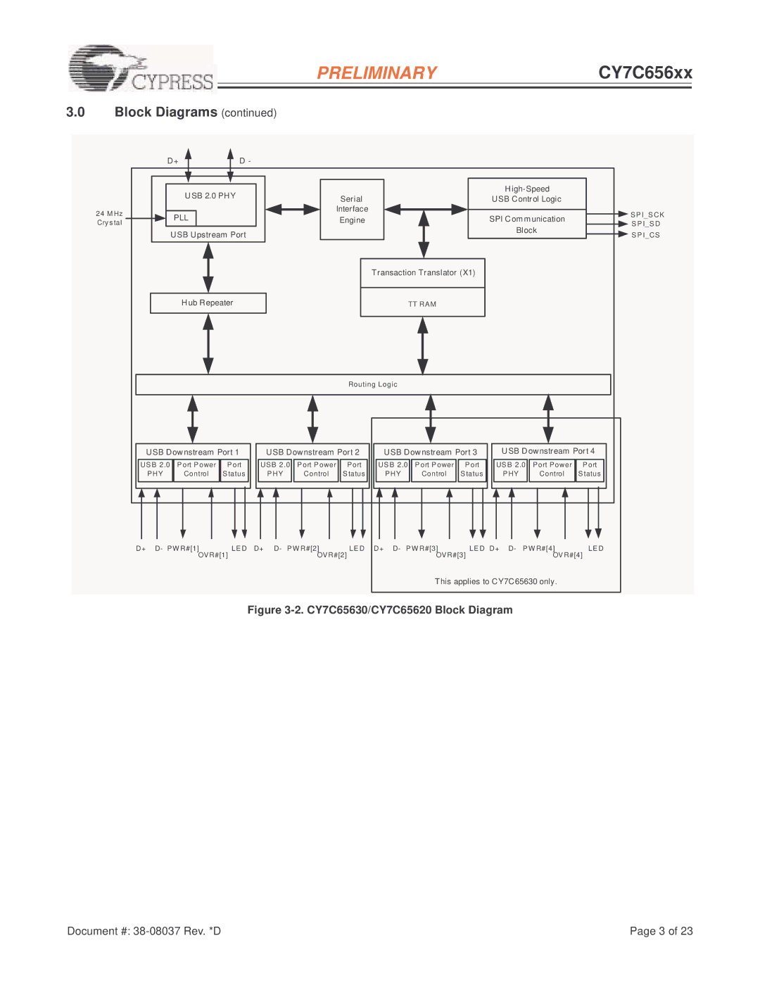
3.0Block Diagrams (continued)
24M Hz Cry s tal
|
|
| D+ |
|
| D - |
|
|
|
|
|
|
|
|
|
| ||||||||
|
|
|
|
|
|
|
|
|
|
|
|
|
|
|
|
|
|
|
|
|
|
|
|
|
|
|
|
|
|
|
|
|
|
|
|
|
|
|
|
|
|
|
|
|
|
|
|
|
|
|
|
|
|
|
|
|
|
|
|
|
|
|
|
|
|
|
|
|
|
| H |
|
|
|
|
|
| U SB 2.0 PHY |
|
|
|
|
|
|
|
|
|
|
|
|
|
|
|
| |||||
|
|
|
|
|
|
|
| Serial |
|
|
|
|
|
| USB Control Logic |
|
|
| ||||||
|
|
|
|
|
|
|
|
|
|
|
|
|
|
|
|
|
|
|
|
|
| |||
|
|
|
|
|
|
|
|
|
|
|
|
| Interface |
|
|
|
|
|
|
|
|
| SP I_S CK | |
|
|
| PLL |
|
|
|
|
|
|
|
| Engine |
|
|
|
|
|
| SPI C om m unication |
|
| |||
|
|
|
|
|
|
|
|
|
|
|
|
|
|
|
|
|
|
| S P I_S D | |||||
|
|
| USB Upstream Port |
|
|
|
|
|
|
|
|
|
|
|
| Block |
|
| S P I_CS | |||||
|
|
|
|
|
|
|
|
|
|
|
|
|
|
|
|
|
|
|
|
|
|
|
|
|
|
|
|
|
|
|
|
|
|
|
|
|
|
|
|
|
|
|
|
|
|
|
|
|
|
|
|
|
|
|
|
|
|
|
|
|
|
|
|
| Transaction Translator (X1) |
|
|
|
| |||||
|
|
|
|
|
|
|
|
|
|
|
|
|
|
|
|
|
|
|
|
|
|
|
|
|
|
|
|
|
|
|
|
|
|
|
|
|
|
|
|
|
|
|
|
|
|
|
|
|
|
|
|
| H ub Repeater |
|
|
|
|
|
|
|
|
| TT RAM |
|
|
|
| |||||||
|
|
|
|
|
|
|
|
|
|
|
|
|
|
|
|
|
|
|
|
|
|
|
|
|
|
|
|
|
|
|
|
|
|
|
|
|
|
|
|
|
|
|
|
|
|
|
|
|
|
Routing Logic
| USB Dow nstream Port 1 |
| USB Downstream Port 2 |
| USB Dow nstream Port 3 |
| U SB D ownstream Port 4 |
| |||||||||||||||||||||||||||||
| US B 2.0 | P ort P ower | P ort |
| USB 2 | .0 | P ort P ower | Port |
| US B 2.0 | P ort P ower | P ort |
| US B 2.0 | Port Power | P ort |
| ||||||||||||||||||||
| PHY |
| Control | S tatus |
| P HY |
|
| Control | S tatus |
| PHY |
| Control | S tatus |
| P HY |
| Control | S tatus |
| ||||||||||||||||
|
|
|
|
|
|
|
|
|
|
|
|
|
|
|
|
|
|
|
|
|
|
|
|
|
|
|
|
|
|
|
|
|
|
|
|
|
|
|
|
|
|
|
|
|
|
|
|
|
|
|
|
|
|
|
|
|
|
|
|
|
|
|
|
|
|
|
|
|
|
|
|
|
|
|
|
|
|
|
|
|
|
|
|
|
|
|
|
|
|
|
|
|
|
|
|
|
|
|
|
|
|
|
|
|
|
|
|
|
|
|
|
|
|
|
|
|
|
|
|
|
|
|
|
|
|
|
|
|
|
|
|
|
|
|
|
|
|
|
|
|
|
|
|
|
|
|
|
|
|
|
|
|
|
|
|
|
|
|
|
|
|
|
|
|
|
|
|
|
|
|
|
|
|
|
|
|
|
|
|
|
|
|
|
|
|
|
|
|
|
D+ D- PW R#[1] | LE D D+ D- P W R#[2] | LE D D+ D- P W R#[3] | LE D D+ D- P W R#[4] | LE D |
OVR#[1] | OVR#[2] | OVR#[3] | OV R#[4] |
|
This applies to CY7C65630 only.
Figure 3-2. CY7C65630/CY7C65620 Block Diagram
Document #: | Page 3 of 23 |