PRELIMINARYCY7C656xx
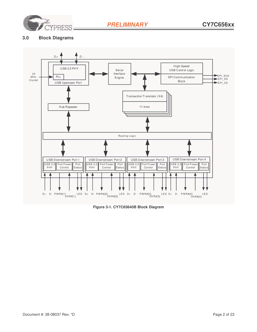
3.0Block Diagrams
24
MHz
Cry s tal
|
| D + | D - |
|
|
|
|
|
|
|
|
|
|
|
|
|
| U SB 2.0 PH Y |
|
|
|
|
|
|
|
|
|
| |||
|
|
|
|
| Serial |
|
|
|
| USB C ontrol Logic |
| ||||
|
|
|
|
|
|
|
|
|
|
|
| ||||
|
| PLL |
|
|
|
| Interface |
|
|
|
|
|
|
| S PI_SCK |
|
|
|
|
|
| Engine |
|
|
|
| SPI Com m unication | ||||
|
|
|
|
|
|
|
|
|
| S PI_SD | |||||
|
|
|
|
|
|
|
|
|
|
|
|
| Block | ||
|
| U SB Upstream Port |
|
|
|
|
|
|
|
|
| S PI_CS | |||
|
|
|
|
|
|
|
|
|
|
|
|
| |||
|
|
|
|
|
|
|
| Transaction Translator (X4) |
|
|
|
| |||
|
| H ub Repeater |
|
|
|
|
|
| TT RAM |
|
|
|
|
| |
|
|
|
|
|
|
| Routing Logic |
|
|
|
|
|
| ||
| U SB Downstream Port 1 |
| USB D ownstream Port 2 |
| USB D ow nstream Port 3 |
| USB D ow nstream Port 4 | ||||||||
US B 2.0 Port P ower | Port | USB 2.0 Port P ower | Port | USB 2.0 | Port P ower | Port | USB 2.0 P ort P ower | Port | |||||||
| P HY | Control | S tatus |
| PHY | Control | S tatus |
| PHY | Control | S tatus |
| PHY | Control | S tatus |
D+ | D- | P W R#[1] | LE D | D+ | D- | P W R#[2] | LE D | D+ | D- | P W R#[3] | LE D | D+ | D- | P W R#[4] | LE D |
|
| OVR#[1] |
|
| OVR#[2] |
|
| OV R#[3] |
|
| OVR#[4] | ||||
|
|
|
|
| Figure |
|
|
|
| ||||||
Document #: | Page 2 of 23 |