Software RECALL
Data is transferred from the nonvolatile memory to the SRAM by a software address sequence. A software RECALL cycle is initiated with a sequence of READ operations in a manner similar to the software STORE initiation. To initiate the RECALL cycle, the following sequence of CE controlled READ operations is performed:
1.Read address 0x0E38, Valid READ
2.Read address 0x31C7, Valid READ
3.Read address 0x03E0, Valid READ
4.Read address 0x3C1F, Valid READ
5.Read address 0x303F, Valid READ
6.Read address 0x0C63, Initiate RECALL cycle
Internally, RECALL is a two step procedure. First, the SRAM data is cleared, and then the nonvolatile information is transferred into the SRAM cells. After the tRECALL cycle time, the SRAM is once again ready for READ and WRITE operations. The RECALL operation does not alter the data in the nonvolatile elements. The nonvolatile data can be recalled an unlimited number of times.
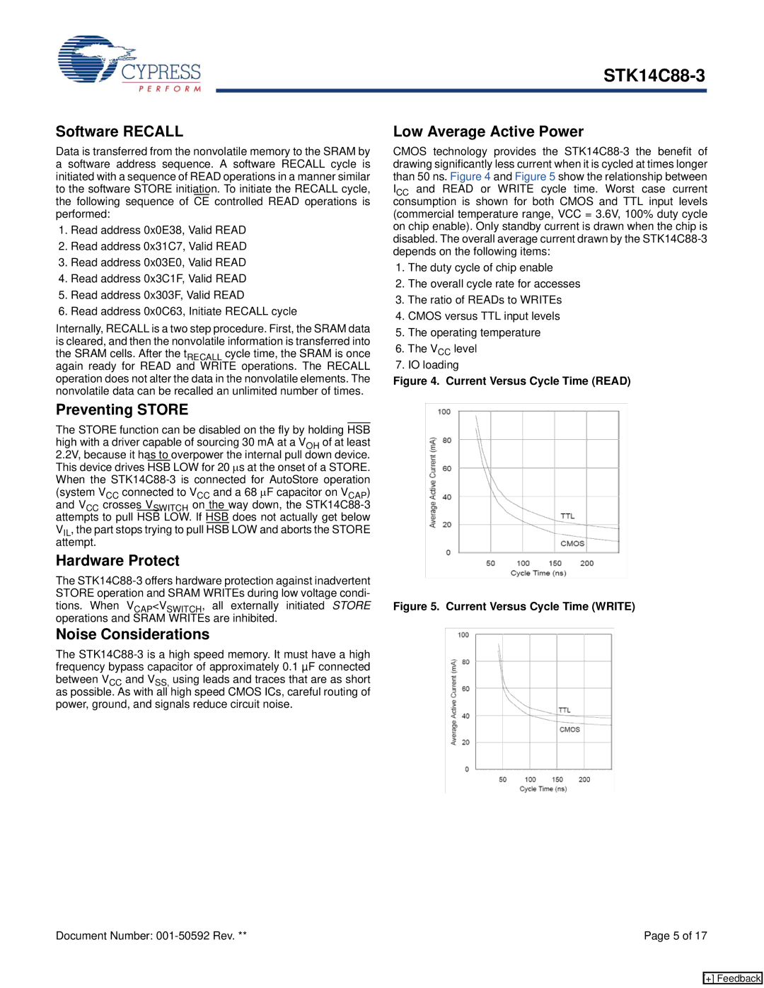
Low Average Active Power
CMOS technology provides the
1.The duty cycle of chip enable
2.The overall cycle rate for accesses
3.The ratio of READs to WRITEs
4.CMOS versus TTL input levels
5.The operating temperature
6.The VCC level
7.IO loading
Figure 4. Current Versus Cycle Time (READ)
Preventing STORE
The STORE function can be disabled on the fly by holding HSB high with a driver capable of sourcing 30 mA at a VOH of at least 2.2V, because it has to overpower the internal pull down device. This device drives HSB LOW for 20 μs at the onset of a STORE. When the
Hardware Protect
The
tions. When VCAP<VSWITCH, all externally initiated STORE Figure 5. Current Versus Cycle Time (WRITE) operations and SRAM WRITEs are inhibited.
Noise Considerations
The
Document Number: | Page 5 of 17 |
[+] Feedback