Pin Configurations
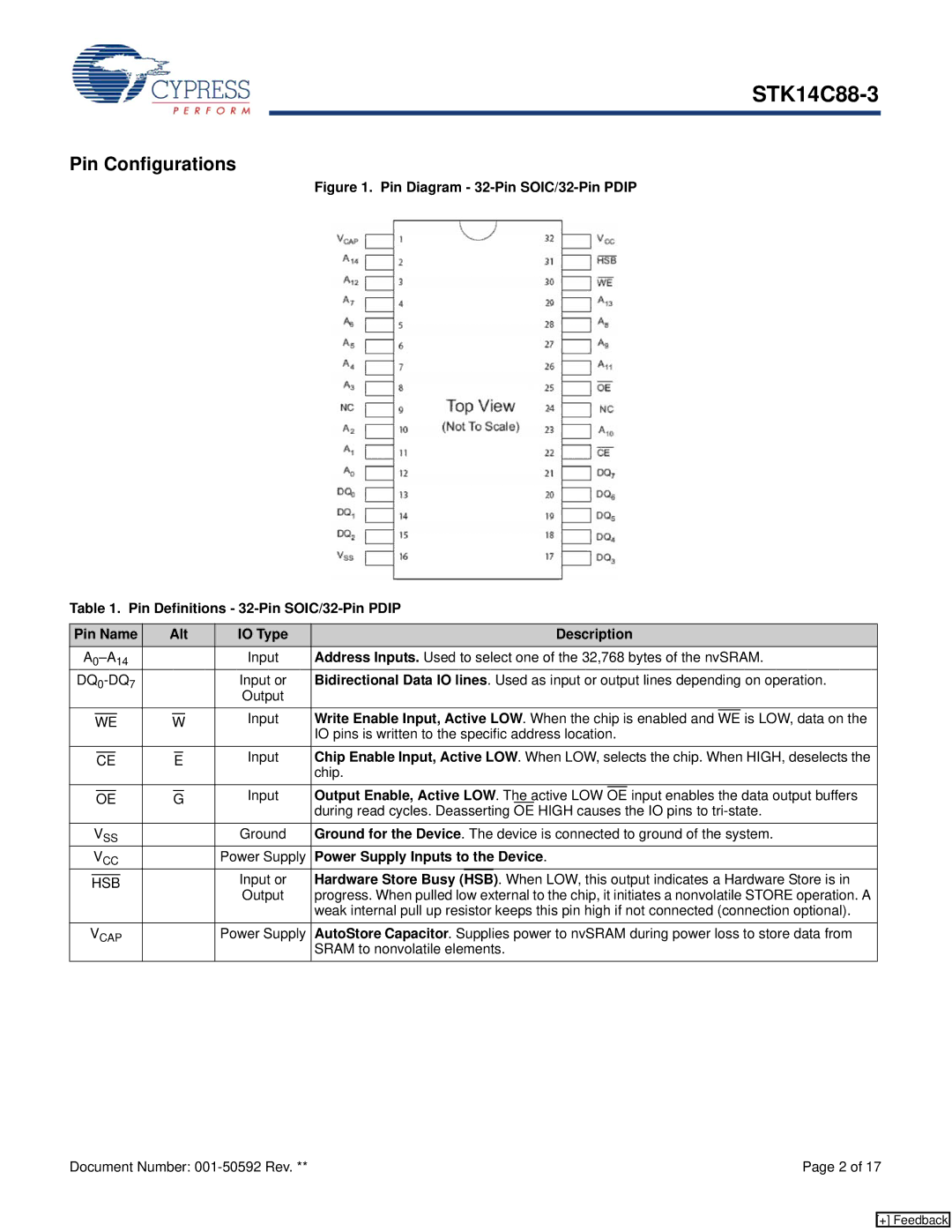
Figure 1. Pin Diagram - 32-Pin SOIC/32-Pin PDIP
Table 1. Pin Definitions - 32-Pin SOIC/32-Pin PDIP
Pin Name | Alt | IO Type |
|
| Description | |||||||||||||||||
|
|
|
|
|
|
| Input | Address Inputs. Used to select one of the 32,768 bytes of the nvSRAM. | ||||||||||||||
|
|
|
|
|
|
| Input or | Bidirectional Data IO lines. Used as input or output lines depending on operation. | ||||||||||||||
|
|
|
|
|
|
|
|
|
|
|
|
|
|
| Output |
|
|
|
|
|
|
|
|
|
|
|
|
|
|
|
|
|
|
|
|
|
| Input | Write Enable Input, Active LOW. When the chip is enabled and |
| is LOW, data on the | ||||
|
|
|
|
|
|
|
|
|
|
|
|
|
|
| WE | |||||||
|
| WE | W | |||||||||||||||||||
|
|
|
|
|
|
|
|
|
|
|
|
|
|
|
| IO pins is written to the specific address location. | ||||||
|
|
|
|
|
|
|
|
|
|
|
|
| Input | Chip Enable Input, Active LOW. When LOW, selects the chip. When HIGH, deselects the | ||||||||
|
|
| CE |
| E | |||||||||||||||||
|
|
|
|
|
|
|
|
|
|
|
|
|
|
|
| chip. | ||||||
|
|
|
|
|
|
|
|
|
|
|
|
|
|
| Input | Output Enable, Active LOW. The active LOW |
| input enables the data output buffers | ||||
|
|
|
|
|
|
|
|
|
|
|
|
| OE | |||||||||
|
| OE |
| G | ||||||||||||||||||
|
|
|
|
|
|
|
|
|
|
|
|
|
|
|
| during read cycles. Deasserting OE HIGH causes the IO pins to | ||||||
| VSS |
|
|
|
|
|
|
| Ground | Ground for the Device. The device is connected to ground of the system. | ||||||||||||
| VCC |
|
|
|
|
|
|
| Power Supply | Power Supply Inputs to the Device. | ||||||||||||
|
|
|
|
|
|
|
|
|
|
|
|
|
|
| Input or | Hardware Store Busy | (HSB) | . When LOW, this output indicates a Hardware Store is in | ||||
| HSB |
|
|
|
|
|
|
| ||||||||||||||
|
|
|
|
|
|
|
|
|
|
|
|
|
|
| Output | progress. When pulled low external to the chip, it initiates a nonvolatile STORE operation. A | ||||||
|
|
|
|
|
|
|
|
|
|
|
|
|
|
|
| weak internal pull up resistor keeps this pin high if not connected (connection optional). | ||||||
VCAP |
|
|
|
|
|
|
| Power Supply | AutoStore Capacitor. Supplies power to nvSRAM during power loss to store data from | |||||||||||||
|
|
|
|
|
|
|
|
|
|
|
|
|
|
|
| SRAM to nonvolatile elements. | ||||||
Document Number: | Page 2 of 17 |
[+] Feedback