STK14C88-5 specifications
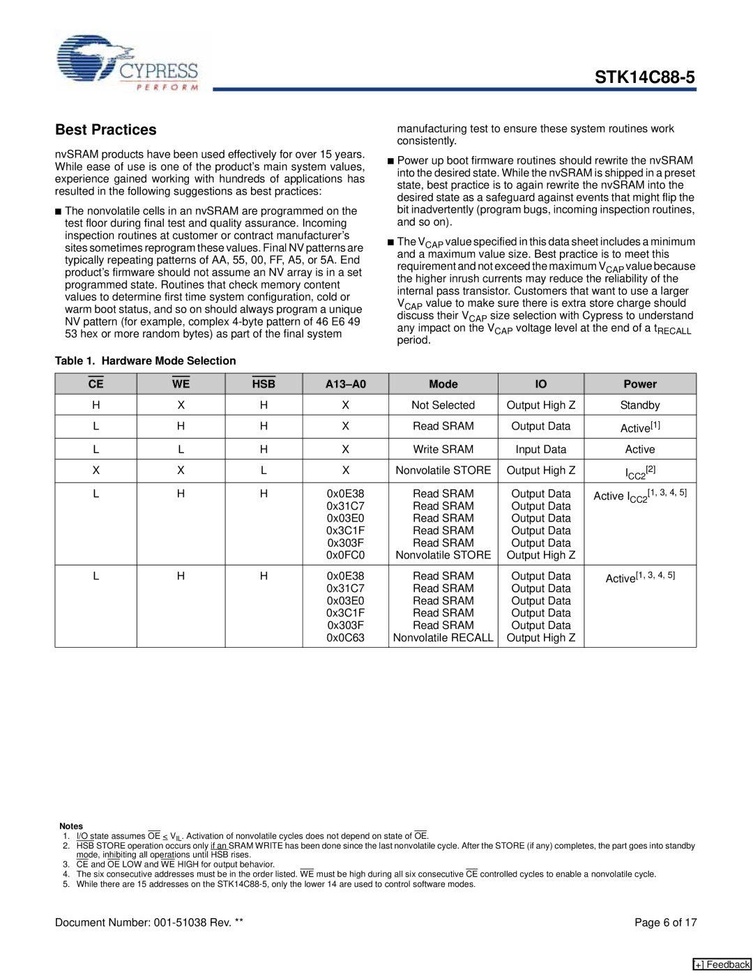
The Cypress STK14C88-5 is a high-performance, non-volatile static random-access memory (SRAM) solution that caters to a wide range of applications. This device seamlessly combines the benefits of SRAM technology with non-volatile memory, making it a compelling option for embedded systems requiring fast access speeds alongside persistent data storage.One of the key features of the STK14C88-5 is its memory density. This chip comes with an 88 Kbit storage capacity, which is ample for various applications, including configuration storage and data logging in industrial systems, telecommunications, and consumer electronics. The memory is organized in a way that supports both byte-wise and word-wise access, ensuring flexibility to accommodate different data structures.
Speed is another attractive characteristic of the STK14C88-5. It operates at access speeds of up to 55 nanoseconds, providing quick read and write capabilities. This rapid performance is crucial for time-sensitive applications, enabling the device to handle real-time data processing effectively. The SRAM also supports a wide operating voltage range from 2.7V to 5.5V, making it versatile for different power supply configurations.
The device utilizes advanced technology to enhance reliability and endurance. The STK14C88-5 features built-in EEPROM technology, which allows it to retain data even when power is lost. This non-volatility is ideal for critical applications where data integrity is paramount.
In terms of interface, the STK14C88-5 provides a simple parallel interface, ensuring compatibility with various microcontrollers and processors. It also has control signals that support straightforward data read and write operations, allowing designers to integrate it easily into their existing architectures.
Moreover, the Cypress STK14C88-5 incorporates low-power consumption features, making it suitable for battery-operated devices. Its efficient power management ensures minimal energy usage without compromising performance, which is crucial in today’s energy-conscious environment.
Overall, the Cypress STK14C88-5 stands out with its combination of non-volatile storage, high-speed access, flexibility of operation, and power efficiency. These features make it an ideal choice for applications that demand reliable memory solutions with fast data processing capabilities, solidifying its position as a valuable component in the semiconductor industry.

