Sty/us Cc#of &mdce Manual
Opemting Principles
2.3.2.1 Reset Circuits
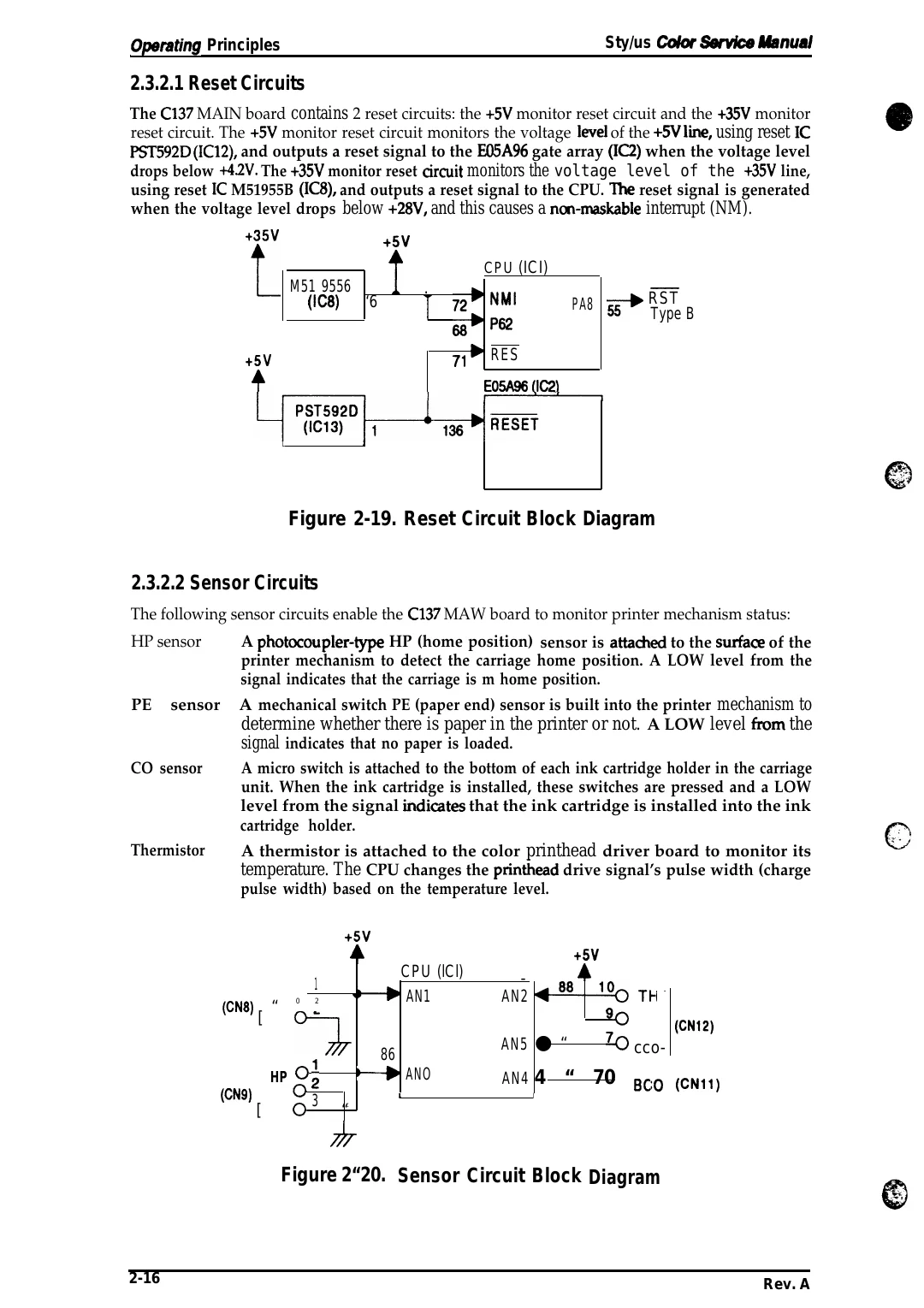
The C137 MAIN board contains 2 reset circuits: the +5V monitor reset circuit and the +35V monitor
reset circuit. The +5V monitor reset circuit monitors the voltage level of the +5V line, using reset IC
PST592D (IC12), and outputs a reset signal to the E05A96 gate array (IQ when the voltage level
drops below +4.2V. The +35V monitor reset arcuit monitors the voltage level of the +35V line,
using reset IC M51955B (IC8), and outputs a reset signal to the CPU. The reset signal is generated
when the voltage level drops below +28V, and this causes a non-maskable interrupt (NM).
+35V
@
+5V
L
CPU (ICI)
M51 9556
(IC8)
‘6
.
PA8 -# RST
Type B
72• NMI
68+ P62
71 b RES
E05A96 (IC2I
+5V
+
L
1
‘. .,-
@
Figure 2-19. Reset Circuit Block Diagram
2.3.2.2 Sensor Circuits
The following sensor circuits enable the C137 MAW board to monitor printer mechanism status:
HP sensor
A photocoupler-type HP (home position) sensor is attachd to the surfam of the
printer mechanism to detect the carriage home position. A LOW level from the
signal indicates that the carriage is m home position.
PE
A mechanical switch PE (paper end) sensor is built into the printer mechanism to
determine whether there is paper in the printer or not. A LOW level hm the
signal indicates that no paper is loaded.
A micro switch is attached to the bottom of each ink cartridge holder in the carriage
unit. When the ink cartridge is installed, these switches are pressed and a LOW
level from the signal indiates that the ink cartridge is installed into the ink
cartridge holder.
sensor
CO sensor
Thermistor
A thermistor is attached to the color printhead driver board to monitor its
temperature. The CPU changes the print&ad drive signal’s pulse width (charge
pulse width) based on the temperature level.
+5V
+5V
CPU (lCl)
1
(CN8)
[
“
0
Y h ~ AN1
2
>
AN5 ● “
86
ANO
HP o ;
(CN9)
[
:
3
-
-
AN2 e ~ TH
90
1
AN4 4
(CN12)
70 cco-
“ 70 ~~o (CN1l)
I
“ : ‘b
h
Figure 2“20. Sensor Circuit Block Diagram
2-16
Rev. A
*.
c;